Comprehensive review on photonic van der Waals integration
Published in Materials
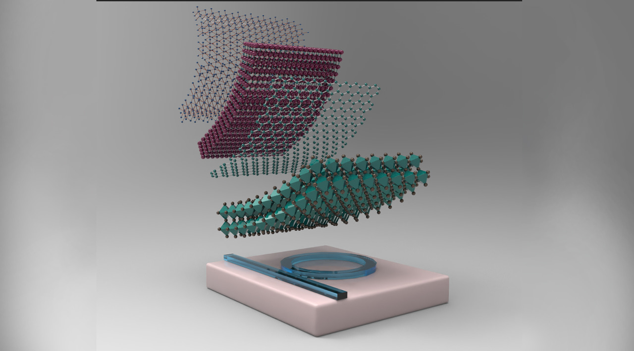
Two-dimensional (3D) materials are well-established building blocks with dangling bond-free film surfaces building van der Waals (vdW) heterostructures and vdW integration [1]. Recent advent on advanced epitaxy and layer lift-off technologies have enabled a wide spectrum of single-crystalline 3D nanomembranes that can also be exfoliated from parent substrate as freestanding form [2-4] with vdW interfaces to facilitate vdW integration with other 2D or 3D nanomembranes.
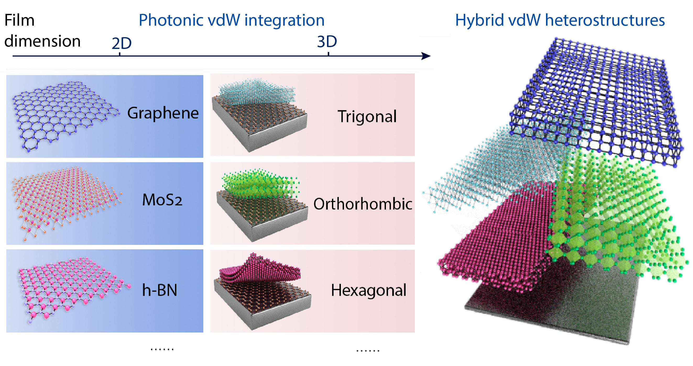
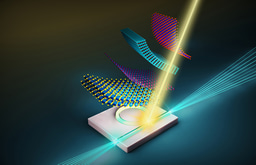
We present a recent survey on latest progress of vdW integration for photonic and optoelectronic applications, encompassing a wide range of 2D and 3D freestanding thin-films and their vdW heterostructures [5, 6]. These vdW building blocks can be transferred and optically couple with diverse photonic structures (Fig. 1) to investigate nanophotonic polaritonic physics [7-9], and permit advanced heterogeneously integrated photonics, without the constraints of lattice matching or process compatibility that apply to heteroepitaxy.
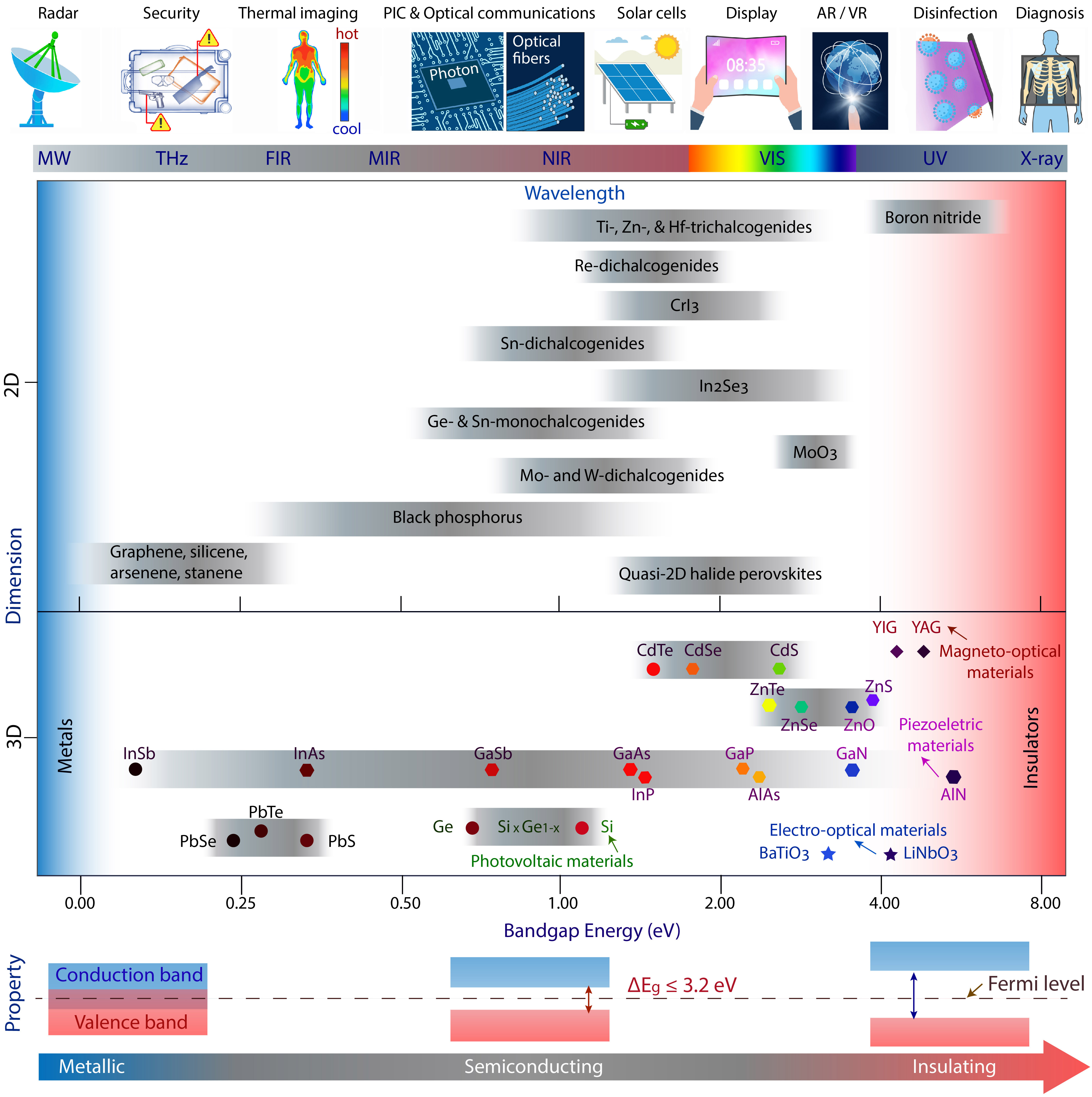
A comprehensive survey from 2D and 3D nanomembranes preparation to device implementation are presented (Fig. 2). Awaiting challenges and emergent opportunities are also outlined based on current perspectives. The detailed information of the Review is appended below. Thank you very much for your reading.
Corresponding authors: Prof. Sang-Hoon Bae (WUSTL), Prof. Cheng-Wei Qiu (NUS), Prof. Lan Yang (WUSTL), Prof. Jin-Wook Lee (SKKU).
Article Information:
Y. Meng, J. Feng, S. Han, et al. Photonic van der Waals integration from 2D materials to 3D nanomembranes, Nature Reviews Materials (2023).
DOI: 10.1038/s41578-023-00558-w
Article link:
https://www.nature.com/articles/s41578-023-00558-w
References:
[1] Y. Liu, et al. Van der Waals integration before and beyond two-dimensional materials, Nature, 567, 323–333 (2019).
[2] H. Kim, et al. Remote Epitaxy, Nature Reviews Methods Primers, 2, 40 (2022).
[3] S. -H. Bae, et al. Integration of bulk materials with two-dimensional materials for physical coupling and applications, Nature Materials, 18, 550–560 (2019).
[4] H. Kum, et al. Epitaxial growth and layer-transfer techniques for heterogeneous integration of materials for electronic and photonic devices, Nature Electronics, 2, 439–450 (2019).
[5] J. A. Rogers, et al. Synthesis, assembly and applications of semiconductor nanomembranes, Nature, 477, 45–53 (2011).
[6] K. S. Kim, et al. Non-epitaxial single-crystal 2D material growth by geometric confinement, Nature, 614, 88–94 (2023).
[7] Z. Dai, et al. Artificial metaphotonics born naturally in two dimensions. Chemical Reviews, 120, 6197–6246 (2020).
[8] L. Shao, et al. Non-reciprocal transmission of microwave acoustic waves in nonlinear parity–time symmetric resonators, Nature Electronics, 3, 267–272 (2020).
[9] H. Lin, et al. Engineering van der Waals materials for advanced meta-photonics. Chemical Reviews, 122, 15204–15355 (2022).
Follow the Topic
-
Nature Reviews Materials

This journal aims to cover the making, measuring, modelling and manufacturing of materials - thus, looking at materials science throughout the pipeline of laboratory discovery to functional device.




Please sign in or register for FREE
If you are a registered user on Research Communities by Springer Nature, please sign in