High-κ monocrystalline dielectrics for low-power two-dimensional electronics
Published in Materials

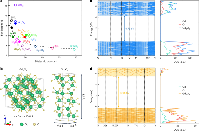
The continued shrinking of the physical feature size of metal-oxide-semiconductor field-effect transistors (MOSFETs) has been the main impetus in the evolution of integrated circuits. Such advances are accomplished through several technology developments including reducing the thickness of channel and gate oxide. In particular, the ideal dielectric with a combination of high dielectric constant (ε ≥ 12) and wide bandgap(Eg ≥ 5 eV) is highly desired. On the one hand, the use of high-κ dielectrics to replace silicon dioxide could greatly reduce the gate leakage and enhance the overall gate controllability on the channel with scaled supply voltage. On the other hand, a wide bandgap allows high dielectric strength and sufficient band offsets (≥ 1 eV) to minimize conduction by the Schottky emission of carriers into the dielectric bands. However, in typical inorganic dielectrics, the bandgap is inversely proportional to the dielectric constant, which is the sum of electronic and ionic contributions, ε = ε∞ + εion. The former, which comes from the reorganization of electronic density, is usually inversely proportional to the bandgap. Thus, any desire to increase the overall dielectric constant in wide-bandgap materials must target the ionic contribution, which depends principally on the crystal structure and the associated vibrational modes, and does not have to follow the above inverse relation.
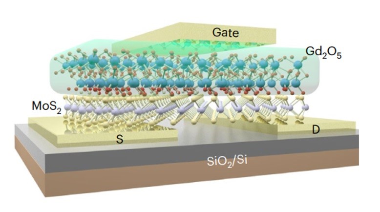
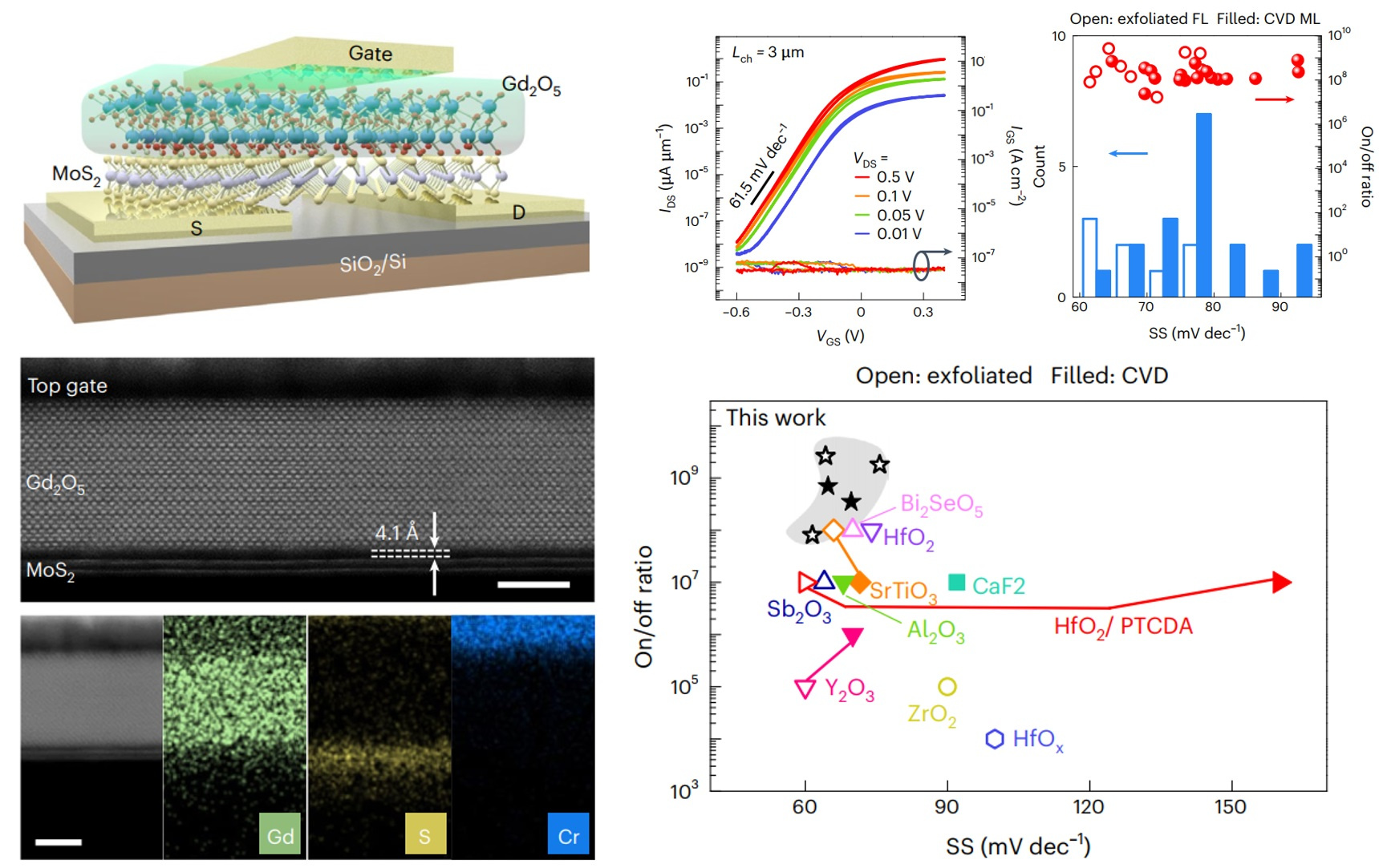
Prof. He’s group successfully synthesized single-crystal 2D gadolinium oxide thin films via van der Waals epitaxy, achieving both high dielectric constant (~25.5) and wide bandgap. Under an electric field of 5 MV cm-1, the 2D gadolinium oxide, with an equivalent oxide thickness as thin as 1 nm, exhibited exceptionally low leakage current (10-4 A cm-2), meeting the IRDS requirements for low-power devices. Furthermore, through van der Waals interactions, seamless integration of single-crystal gadolinium oxide with 2D semiconductors was achieved. The high-κ dielectric environment and high-quality gate dielectric/semiconductor interface enabled the fabricated 2D transistors to demonstrate exceptional modulation capabilities under low operating voltages, featuring an on/off ratio exceeding 109, a subthreshold swing approaching the Boltzmann physical limit, and effective suppression of short-channel effects. The inverter circuits constructed by the low-power 2D transistors achieved a gain of 40 and an ultra-low power consumption of merely 3.5 nW.

Follow the Topic
-
Nature Materials
A monthly multi-disciplinary journal that brings together cutting-edge research across the entire spectrum of materials science and engineering, including applied and fundamental aspects of the synthesis/processing, structure/composition, properties and performance of materials.


Please sign in or register for FREE
If you are a registered user on Research Communities by Springer Nature, please sign in