Unveiling the carrier dynamics of a coplanar 2D heterojunction via time-resolved photoemission electron microscopy
Published in Electrical & Electronic Engineering

Electrical control of charge carrier flow is the foundation of modern electronics. Two-dimensional (2D) semiconducting materials become particularly attractive in next-generation electronic device applications due to their atomic thickness and nonzero bandgap. Efforts towards constructing high-performance 2D electronic and optoelectronic devices require a fundamental understanding of the carrier dynamics. The time-resolved photoemission electron microscopy (TR-PEEM)1 can simultaneously access the evolution of electrons on the time, space, and energy, providing a direct way to image the carrier dynamics of semiconductor devices. Since, in most of the semiconductor devices, carriers transport in the in-plane structures, it is of considerable significance to image the carrier injection and transport in the 2D limit. However, the electron relaxation and motion in the 2D limit in-plane structure has seldom been reported.
In the way to the scaling in integrated circuits, the electrical contacts that connect to the 2D semiconductors become critical and affected the performance of the electronic and optoelectronic devices significantly. The typical direct metal electrode deposition can introduce defects and impurities, leading to a reduction of the performances. Recently, contacting 2D semiconductors through seamless coplanar 2D metal, for instance, 1T′/2H MoTe2 heterojunction, has been developed. This seamless coplanar 2D metal/semiconductor structure via covalent bonds can significantly reduce the contact resistance2, and also provide an ideal platform to study the electron relaxation and motion in in-plane structure.
Here, we investigated the electron dynamics in energy, time, and space dimensions at a coplanar 1T′/2H-MoTe2 heterojunction by employing the TR-PEEM technique (Fig. 1a). After the excitation by 3.02 eV pump light, the photoexcited electrons are accessible by a 4.54 eV probe light (purple region) (Fig. 1b and 1c). The non-equilibrium photoexcited electrons distributed and evolved heterogeneously near the heterojunction interface. The photoexcited electrons in the 1T′-MoTe2 region possessed higher energy compared with that in the 2H-MoTe2 region (Fig. 1d). And the energy of the non-equilibrium electrons collapsed and relaxed rapidly to the lower energy levels on several picoseconds timescale (Fig. 1e). At the metal/semiconductor interface, the photoexcited electrons in the 1T′-MoTe2 region decay faster than that of the 2H-MoTe2 region (Fig. 1f). That could be due to the charge transport or energy transfer with a rate of about 0.80×10¹² s−1. The results are useful for the design and fabrication of high-performance 2D electronic and optoelectronic devices.
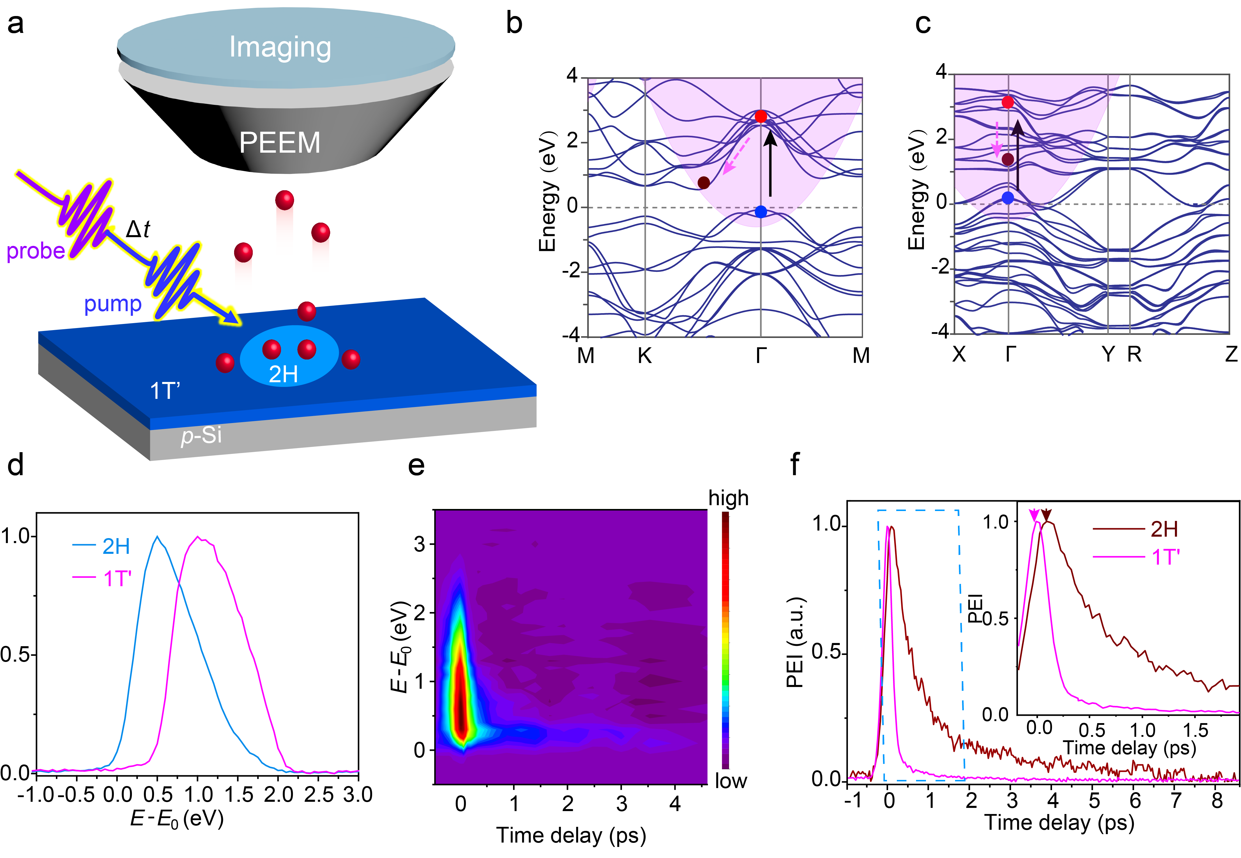
Fig. 1 a Schematic of the TR-PEEM setup. b, c The probe window (purple regions) of the band structure of a bilayer 2H (b) and 1T′ (c) MoTe2. d Normalized photoelectron spectroscopy illuminated by the 410 nm pulsed laser. ′E-E0′ indicates the kinetic energy of the electrons. e Mapping of photoemission intensity (PEI) versus the delay time and kinetic energy. f Time traces of the PEIs. Inset: enlarging the curves within ~2 ps.
Reference
1 Man, M. K. et al. Nat. Nanotechnol 12, 36-40 (2017).
2 Xu, X. et al. J. Am. Chem. Soc. 141, 2128-2134 (2019).
Follow the Topic
-
Communications Materials
A selective open access journal from Nature Portfolio publishing high-quality research, reviews and commentary in all areas of materials science.

Related Collections
With Collections, you can get published faster and increase your visibility.
Smart windows for sustainable buildings
Publishing Model: Open Access
Deadline: Oct 31, 2026
Lead-free perovskite solar cells
Publishing Model: Open Access
Deadline: Oct 31, 2026


Please sign in or register for FREE
If you are a registered user on Research Communities by Springer Nature, please sign in