Visualization of excitons trapped in a nanoscale pattern
Published in Physics


Moiré pattern
Have you ever looked through two thin curtains hanging one behind the other and noticed broad wavy patterns to appear? You may have noticed similar wavy bands when taking a close-up photo of a computer or television screen. In both cases, two fine repeating patterns that are slightly misaligned overlap. This overlap creates a much larger visible pattern, which is known as a moiré pattern, see Fig. 1.
Physicists from the Netherlands, together with collaborators from Brazil and Japan, used this principle in an extremely thin semiconductor. They stacked two thin layers of molybdenum disulfide (MoS2) and rotated one layer by about two degrees with respect to the other layer. This small twist led to the formation of a repeating nanoscale moiré pattern that changes how light interacts with the material and revealed that light-induced excitations are trapped at specific locations within this pattern [1]. Their findings could contribute to the development of extremely small optoelectronic devices.
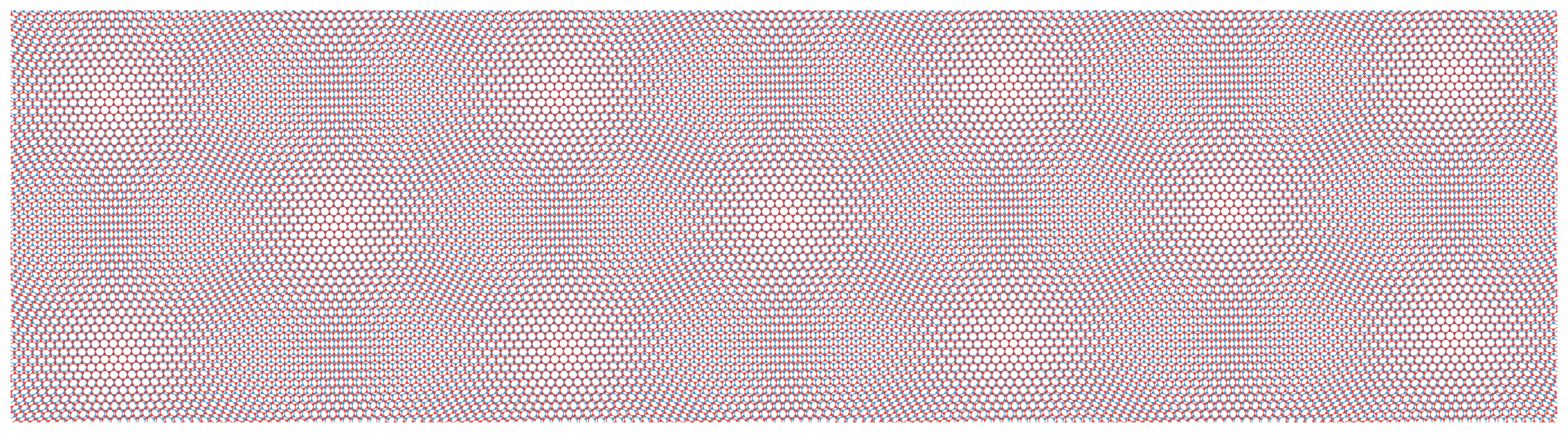
Fig. 1: Moiré pattern that forms when two lattice grids overlap in a misaligned way.
Excitons
Like cars in a high parking tower, which start occupying the lowest floors and let the highest floors empty, electrons in a material will systematically fill up the lowest energy levels available and let the highest levels empty. However, by shining light in a material, some electrons in the lowest filled levels get enough energy to be excited to a higher empty level. Contrarily to cars, the electrons that get excited to higher energies leave behind an empty place (hole), which is positively charged. The electron and the hole then bind through their electrostatic interaction and form an exciton - an electron-hole bound pair [2], see Fig. 2. Another property that differentiates electrons from cars is that electrons have an intrinsic magnetic moment, a so-called spin. For materials that have a strong spin-orbit coupling, as is the case for molybdenum disulfide, there are different ways to pair up electrons and holes. This leads to different excitonic species, which are, very creatively, called Exciton A, Exciton B, etc. In addition, they may even form bi-excitons (two bound excitons) or a trion, an exciton bound to another electron or hole.
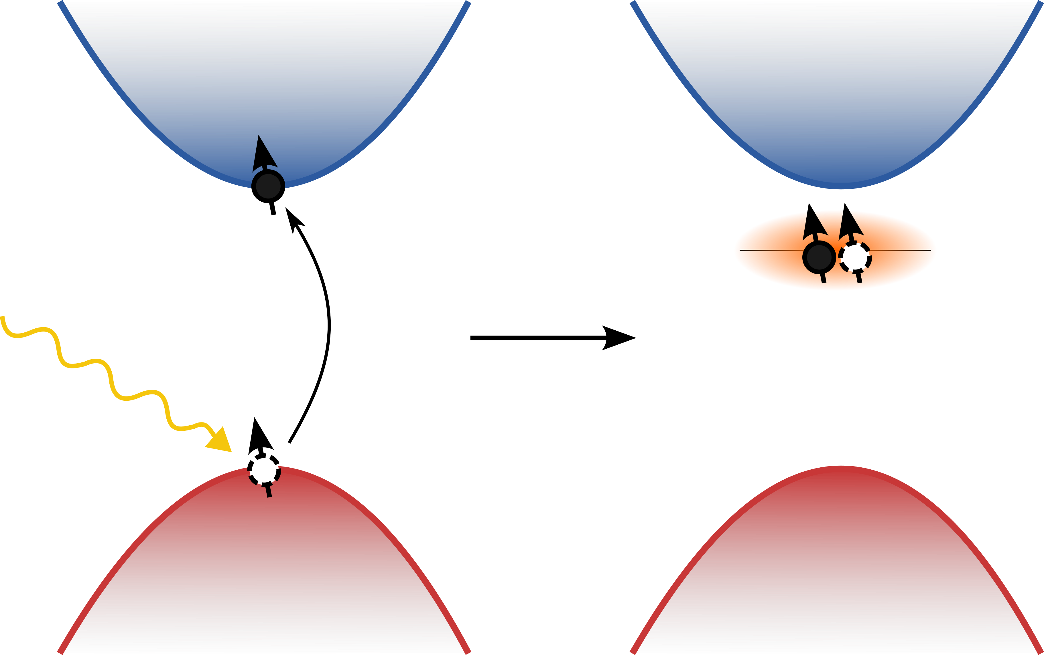
Fig. 2: Exciton formation in solid-state materials: The energy bands in red are filled up with electrons, and the blue ones are empty. By shining light in the material, electrons from the red low-energy (valence) band are excited to the blue high-energy (conduction) band and leave a hole behind. The hole and the electron form a bound state known as exciton.
Although we can know very well the energy of the excitons that form when we shine light in the material, until now we have not been able to fully “see” the excitons in real space [1,3,4]. State of the art microscopy techniques can resolve individual atoms, and previous studies have mapped excitonic responses with high spatial resolution [3,4]. The challenge is to combine spatial information with energy resolution so that different excitonic states can be distinguished within the same nanoscale structure. Moiré patterns make this especially interesting because their periodicity is much larger than that of the underlying atomic lattice, typically several nanometres rather than a few ångströms.
Twisted bilayers and emergent moiré patterns
The isolation of graphene showed that stable crystals only one atom thick could be produced. Stacking two such layers with a controlled relative rotation creates a much larger moiré superlattice [5]. The same principle applies to other layered materials, including MoS₂, and makes the twist-induced pattern accessible to scanning-probe microscopy.
Here, the team used molybdenum disulfide [1,6], a two-dimensional material similar to graphene, which is however 3-atoms thick. By twisting two layers of them on top of each other with an angle of two degrees, a moiré pattern emerges, with a lattice of the order of nanometers (10-9m). Concerning the energy landscape, each layer has an energy structure for the electrons like the parking tower discussed earlier. When two layers are stacked, the energy levels of different layers get intertwined, and by shining light on the sample it is now possible to form not only intra-layer excitons, but also inter-layer excitons, when electrons from the filled energy levels of one layer go to the empty levels of another layer. The problem becomes richer and more complex, but there is one advantage: the excitons are now formed on the larger moiré lattice and could in principle be directly visualized.
Real-space observation of excitons
Researchers in Pantelis Bampoulis’s group at the University of Twente mapped this response using photocurrent atomic force microscopy. Laurens Westenberg scanned the stacked layers with an atomically sharp conductive tip while illuminating the sample from below with precisely tuned photon energies (Fig. 3). At each position, the tip measured the light-induced current, allowing the team to map where light energy is absorbed. Repeating the scan across different photon energies produced maps showing where the photoresponse associated with each excitonic resonance was strongest [1].
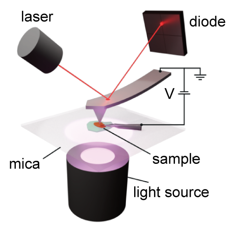
Fig. 3: Sketch of the experimental setup. Taken from Ref [1].
Although earlier studies had already provided evidence for moiré-trapped excitons [3,4,7], something really new was obtained in this work by controlling the energy of the light shone on the sample: different kinds of excitons gather at different spots within the pattern. Intralayer excitons sit at positions where molybdenum atoms in different layers align (which we call RMM regions in Fig. 4). In contrast, interlayer excitons reside at the border between these neighbourhoods (which are called bridges in Fig. 4). Each exciton stays confined to a spot of roughly two nanometres.
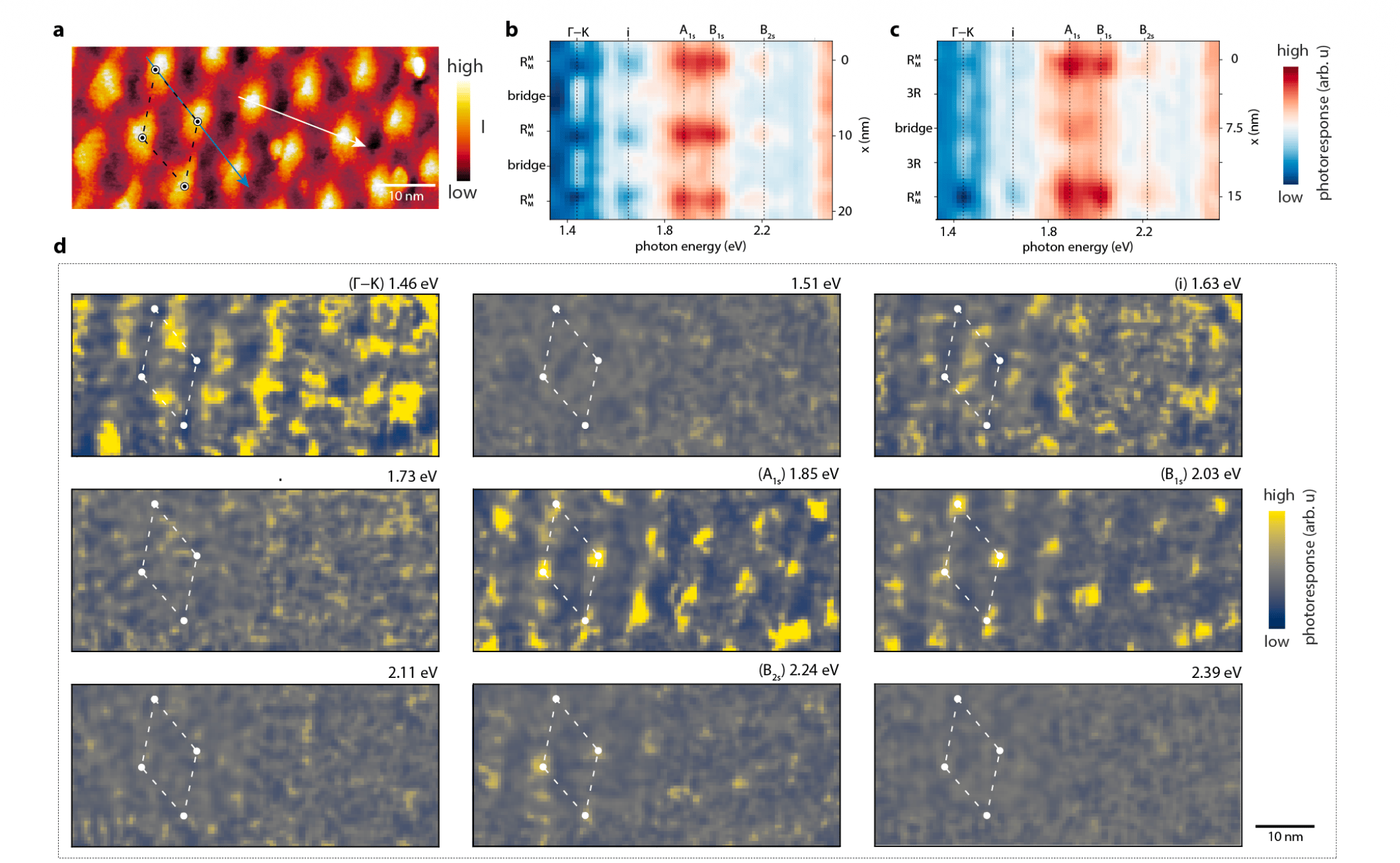
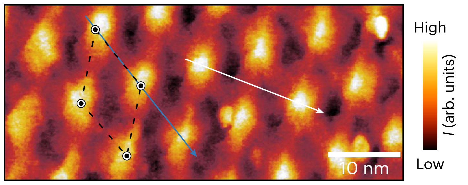
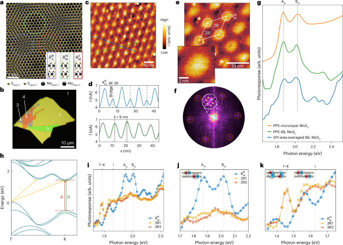
Figure 4. Energy- and position-resolved photoresponse of twisted bilayer MoS₂. (a) Current map of the moiré lattice; arrows show the scan paths. (b,c) Photoresponse as a function of position and photon energy along the blue and white paths, respectively. (d) Maps at selected photon energies show that direct A/B excitons and indirect excitonic features are strongest at different stacking regions. Adapted from Fig. 2 of Ref. [1].
Theory explains how the excitons are trapped
Although excitons are tiny by everyday standards, they are large compared with individual atoms: their quantum-mechanical wavefunction can extend across many atomic sites. They are also normally free to move through a material. How, then, can the moiré pattern confine them to regions only two nanometres wide?
To answer this question, theoretical physicist Lumen Eek in the group of Cristiane Morais Smith at Utrecht University, in collaboration with Rodrigo Arouca at the Brazilian Centre for Research in Physics modelled the excitons in the twisted layers. Because the arrangement of the atoms varies across the moiré pattern, the energy of this pair also changes from place to place. The resulting energy landscape contains a repeating pattern of hills and valleys. Excitons tend to move towards the valleys, where their energy is lowest, and become trapped there.
The model reproduced very well the exciton energies measured in the experiment. It also showed that bright, direct excitons concentrate around the crossing points of the moiré lattice, in regions a few nanometres wide, whereas indirect excitons concentrate at the lattice bridges. The theory therefore connects the patterns in the experimental images to the underlying quantum mechanics and explains why different excitons settle in different places [1].
Towards ultrasmall light sources
Excitons largely determine how the material absorbs and emits light [2]. Scientists have long suspected that a moiré pattern can trap excitons at fixed positions, which would offer a way to control light in a programmable grid [8]. Such control could eventually be useful for very small light sources and, potentially, single-photon emitters.
Earlier studies had already found evidence that moiré patterns can trap excitons [3,4,7]. However, these experiments were limited by spatial averaging, cryogenic operation or sensitivity to only one response. The present method distinguishes several excitonic species within an individual moiré cell at room temperature.
“What is particularly exciting is that we can directly test our microscopic picture of moiré excitons. By connecting the measured real-space patterns to different exciton species, we can understand why and where they localize within the moiré unit cell. This brings us closer to designing excitonic states in twisted materials”, says Lumen Eek.
Working at room temperature is important for possible applications. The measurements show where different excitonic states are concentrated within the moiré pattern, providing information that could help researchers design materials in which light and electronic excitations are controlled on a scale of only a few nanometres. Changing the twist angle also changes the size of the moiré pattern, providing a way to tune the spacing between these regions. “Our results could help with the design of devices that manipulate light absorption with much greater precision,” says Laurens Westenberg [1].
About the researchers
Laurens Westenberg is the PhD student behind the experiments. He is supervised by Dr. Pantelis Bampoulis, an expert in low-dimensional materials and scanning probe microscopies. Bampoulis’s group uses state-of-the-art microscopes to image how electrons and light behave in these materials. His research is funded by an NWO Vidi grant and an ERC grant. Westenberg and Bampoulis work at the MESA+ Institute for Nanotechnology of the University of Twente.
Lumen Eek is a PhD student in the group of Cristiane Morais Smith engaged in the framework of the Gravitation Project QuMat, Materials for the Quantum Age. Rodrigo Arouca is a previous member of the Morais Smith group and currently works at the Brazilian Centre for Physics Research in Rio de Janeiro, Brazil.
The study ‘Real-Space Imaging of Moiré-Confined Excitons in Twisted Bilayer MoS2’ has been published in Nature Physics. University of Twente PhD student Laurens Westenberg performed the experiments. The theoretical model was developed at Utrecht University and the Brazilian Centre for Research in Physics. The supporting boron nitride crystals were grown and characterized at the National Institute for Materials Science in Japan. This international collaboration between researchers in the Netherlands, Brazil and Japan grew out of QuMat (Materials for the Quantum Age), a Dutch Gravitation research program that brings together scientists working on quantum materials.
References
[1] Westenberg, L. J. M. et al. Real-space imaging of moiré-confined excitons in twisted bilayer MoS₂. Nature Physics (2026).
[2] Mueller, T. & Malic, E. Exciton physics and device application of two-dimensional transition metal dichalcogenide semiconductors. npj 2D Materials and Applications 2, 29 (2018).
[3] Susarla, S. et al. Hyperspectral imaging of exciton confinement within a moiré unit cell with a subnanometer electron probe. Science 378, 1235–1239 (2022).
[4] Li, H. et al. Imaging moiré excited states with photocurrent tunnelling microscopy. Nature Materials 23, 633–638 (2024).
[5] Andrei, E. Y. & MacDonald, A. H. Graphene bilayers with a twist. Nature Materials 19, 1265–1275 (2020).
[6] Huang, D., Choi, J., Shih, C.-K. & Li, X. Excitons in semiconductor moiré superlattices. Nature Nanotechnology 17, 227–238 (2022).
[7] Seyler, K. L. et al. Signatures of moiré-trapped valley excitons in MoSe₂/WSe₂ heterobilayers. Nature 567, 66–70 (2019).
[8] Yu, H., Liu, G.-B., Tang, J., Xu, X. & Yao, W. Moiré excitons: From programmable quantum emitter arrays to spin–orbit-coupled artificial lattices. Science Advances 3, e1701696 (2017).
Follow the Topic
-
Nature Physics
This journal publishes papers of the highest quality and significance in all areas of physics, pure and applied.


Please sign in or register for FREE
If you are a registered user on Research Communities by Springer Nature, please sign in