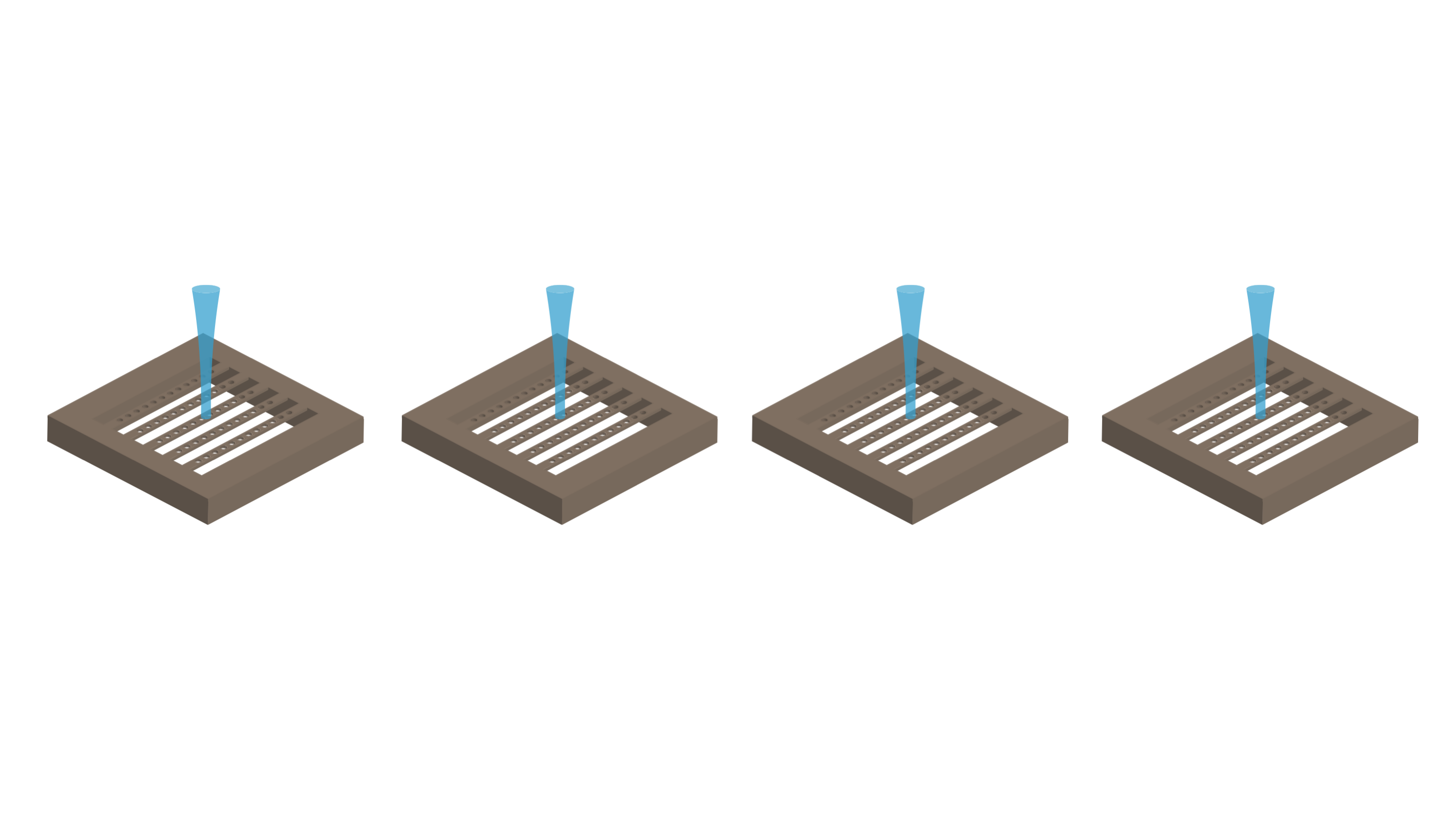
Have you ever wondered how we might make quantum computing, sensing, and communication a reality? Solid-state spin defects are promising tools in making these applications possible. For example, being able to measure a defect’s spin state is key to understanding how the spin is interacting with its environment—as is the goal of quantum sensing [1]. Additionally, if we can read out and store this important spin information, we can build the spin-dependent optical interfaces and quantum memories needed for quantum communication networks [1].
Motivations and First Questions
As is probably evident, defects can play a central role in many quantum applications. Defects are normally integrated into materials via ex-situ focused ion beams and masked ion implantation [2,3]. Our group works closely with the widely-studied silicon monovacancy (VSi(-)) and neutral divacancy (VSiVC(0)) found in 4H-silicon carbide (SiC). Our workflow involves fabricating photonic crystal cavities (PCCs) in SiC and having companies implant defects into our cavities to enhance the defects’ optical properties through the Purcell effect. The Purcell effect is a phenomenon that occurs when a light-emitting atom or atom-like structure (in our case, a defect) is resonantly coupled to a cavity, resulting in faster and enhanced emission of light from the defect (e.g. [4]).
Over the years of sending our devices to external companies for defect implantation, the same question was always lurking in our group: is there a better way to make defects? Specifically, we wondered if we could develop a defect formation method that is more accessible to university research groups (which likely don’t have ion implanters lying around) and can repeatedly incorporate high-quality, single emitters into the centers of nanophotonic cavities. With ex-situ techniques, researchers can only hope that the conditions they requested for ion implantation result in desirable defects. As a result, an improved approach would also include the ability to instantly tailor defect generation conditions to minimize wasted samples and time. In search of such a method, we explored the use of above-bandgap nanosecond laser pulses to laser write defects in nanophotonics for the first time.
Using this accessible, laser-based approach, we successfully integrated spin defects into our PCCs. This laser writing technique not only allows us to overcome the challenges posed by ex-situ methods (waiting for samples to return, large-scale data collection to characterize implanted defects, post processing, etc.), but it also offers a new, high-throughput way to couple defects to photonic structures, supporting the development of defect-based quantum networks.
We were initially inspired by efforts to laser write defects in 4H-SiC using below-bandgap femtosecond laser pulses (e.g. [5]). Wanting to overcome the low emitter yield and optical instability of laser written defects in previous work, we began brainstorming. Our decision to try above-bandgap laser pulses directed at photonic structures stemmed from the fact that no one had ever done so before. Many previous laser writing attempts involved ultra-short, below-bandgap pulses directed at bulk material [5-7].
The logic behind using quick, below-bandgap pulses to excite wide-bandgap materials is that these pulses can induce the simultaneous absorption of many photons in a short amount of time. While this approach can work, we wondered if we could take advantage of the fact that 4H-SiC has a smaller bandgap than other wide-bandgap semiconductors, such as diamond. Due to this property, there are economical above-bandgap lasers that can be used to excite carriers directly across SiC’s bandgap, possibly letting us transfer energy to the material via a more efficient and less damaging process than if we were just limited to the multi-photon absorption described above.
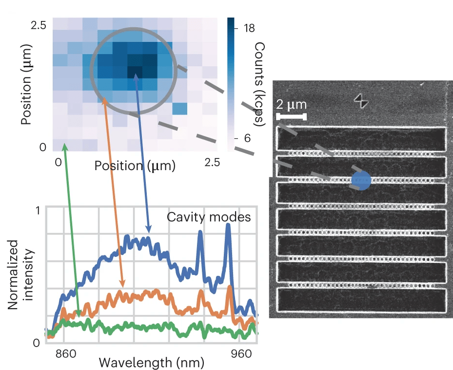
While we had just a hunch for how our defects might be created, we were certain from the start about how we would assess them. Previous work emphasizes that PCCs can act as useful probes of defects’ properties and environments [4]. If our method proved capable of making high-quality defects in a spatially-controlled manner, our PCCs would provide us with clear confirmation: when a defect is placed near the center of a cavity’s mode volume, it can couple to the cavity’s modes, resulting in a photoluminescence (PL) spectrum containing an enhanced defect signature surrounded by cavity modes (e.g. Fig. 1).
Initial Approach
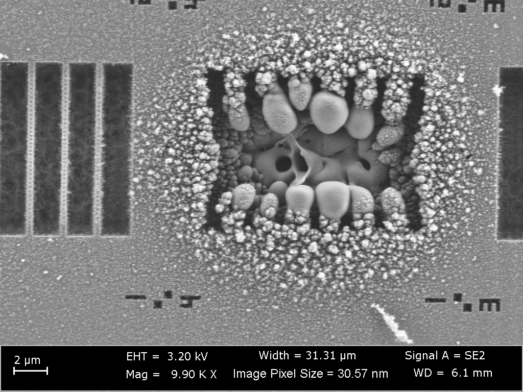
It’s worth noting that we did try below-bandgap pulses, but we couldn’t find a regime where the PCCs remained intact after irradiation (Fig. 2). Interestingly, in the first experiments with our above-bandgap laser, we hoped to see material damage. Our thought process was as follows: if we could induce visible material damage, then maybe we could apply lower-fluence pulses to induce atomic damage to the crystal lattice, resulting in defects while still preserving the macroscopic properties of the material.
Our line of reasoning proved valid, as we eventually found laser conditions under which VSi(-) was created. Though this was a feat in itself, we wanted to pursue more experiments to take advantage of the ease with which we could adjust and evaluate our laser-based process. We quickly realized that, unlike traditional defect generation techniques, we could perform PL measurements on our emitters as soon as they were created and easily tune following experiments based on what we saw.
Finalized Approach and Findings
After seeing that the creation of VSi(-) with our technique was possible, new questions arose: Are there conditions that consistently generate single emitters in SiC? How are emitters interacting with the cavities? Can we glean anything new about the defect formation process (e.g. is there a relationship between irradiation conditions and emitter characteristics)?
We varied the number of pulses along with their fluence and created arrays of irradiated spots to explore these questions. We found that using single pulses with fluences between 0.4–0.9 μJ generated VSi(-) within a cavity-mode volume. Seeing as cavity modes are present pre- and post-irradiation, we were able to integrate VSi(-) into PCCs while preserving the photonic properties of the cavities (Fig. 3).
To better understand the efficiency of and damage imparted by our process, we studied the lifetimes of laser-written emitters. Across various pulse numbers and fluences, we noted short and long decay components for each emitter. By comparing irradiated cavities with an unirradiated cavity, we attributed the short decay component to intrinsic surface defects. Contrastingly, the long decay component appeared dependent on irradiation conditions. After seeing the long decay component shorten when multiple pulses and higher fluences were used, we reasoned that lattice damage is taking place at these conditions, which negatively affects the optical properties of laser-written emitters.
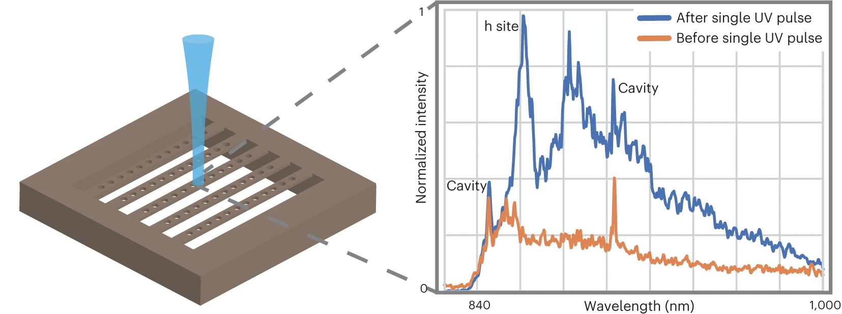
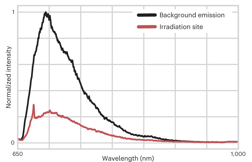
The lifetime data we collected indicated that laser writing produced emitters other than those we were interested in. Wanting to identify the defects, we attempted to excite them. While characterizing, we were very surprised to find a massive reduction in PL for irradiated cavities as compared to unirradiated cavities (Fig. 4). We had unintentionally found a regime where laser irradiation reduced the emission of intrinsic surface defects: electronic states near the surface of a material that give rise to broad background emission in a PL measurement, worsening the signal to noise ratio. After observing this laser annealing, we hope to conduct future experiments that prioritize annealing unwanted surface defects. With this ability, we can overcome the challenges posed by poor-quality host materials, which can degrade emitter properties and limit a device’s utility in a quantum network.
Through these experiments, we were not only able to better understand the physical mechanism of our laser writing process, but also find strong evidence that our method yields high-quality, single emitters that can be coupled to optical cavities. As a result, above-bandgap laser writing can be a useful tool in realizing defect-based quantum communication systems. We hope that our novel method, with its near real-time feedback, tunable nature, and accessibility as a laser-based process, enables other groups to laser write nanophotonics for quantum applications.

References
- Wolfowicz, G., Heremans, F.J., Anderson, C.P. et al. Quantum guidelines for solid-state spin defects. Nat Rev Mater 6, 906–925 (2021). https://doi.org/10.1038/s41578-021-00306-y
- He, Z.-X., Li, Q., Wen, X.-L., Zhou, J.-Y., Lin, W.-X., Hao, Z.-H., Xu, J.-S., Li, C.-F., & Guo, G.-C. (2022). Maskless Generation of Single Silicon Vacancy Arrays in Silicon Carbide by a Focused He + Ion Beam. ACS Photonics. https://doi.org/10.1021/acsphotonics.2c01209
- Schröder, Tim, et al. “Scalable Focused Ion Beam Creation of Nearly Lifetime-Limited Single Quantum Emitters in Diamond Nanostructures.” Nature Communications, vol. 8, no. 1, 2017, pp. 15376–15376, https://doi.org/10.1038/ncomms15376.
- Bracher, David O., et al. “Selective Purcell Enhancement of Two Closely Linked Zero-Phonon Transitions of a Silicon Carbide Color Center.” Proceedings of the National Academy of Sciences - PNAS, vol. 114, no. 16, 2017, pp. 4060–65, https://doi.org/10.1073/pnas.1704219114.
- Chen, Yu-Chen, et al. “Laser Writing of Scalable Single Color Centers in Silicon Carbide.” Nano Letters, vol. 19, no. 4, 2019, pp. 2377–83, https://doi.org/10.1021/acs.nanolett.8b05070.
- Almutairi, A. F. M., et al. “Direct Writing of Divacancy Centers in Silicon Carbide by Femtosecond Laser Irradiation and Subsequent Thermal Annealing.” Applied Physics Letters, vol. 120, no. 1, 2022, p. 14003, https://doi.org/10.1063/5.0070014.
- Castelletto, S., et al. “Photoluminescence in Hexagonal Silicon Carbide by Direct Femtosecond Laser Writing.” Optics Letters, vol. 43, no. 24, 2018, pp. 6077–80, https://doi.org/10.1364/OL.43.006077.
Follow the Topic
-
Nature Materials
A monthly multi-disciplinary journal that brings together cutting-edge research across the entire spectrum of materials science and engineering, including applied and fundamental aspects of the synthesis/processing, structure/composition, properties and performance of materials.






Please sign in or register for FREE
If you are a registered user on Research Communities by Springer Nature, please sign in