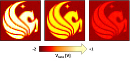
Semiconducting 2D materials such as transition metal dichalcogenides are beginning to generate a lot of interest as a candidate for ultra thin body electronics and optoelectronics. There have been significant advances in the last 2 to 3 years and a shift from papers reporting fundamental properties of these materials towards proof of concept devices and high quality, larger scale synthesis. In technology speak one could say the field has graduated into a Technology Readiness Level of 3-4 where scientists all over the world are conducting research to understand feasibility of using these materials in electronics and optoelectronic components.
This is rapid progress indeed but the jump to TRL 5-6 will require clear understanding of all facets of the device fabrication and integration in order to preserve the figures of merit such as the mobility, subthreshold swing, responsivity and luminescence quantum yield. R&D would therefore need to focus on optimizing each step of device fabrication :
- Growth/deposition of 2D materials
This is the first and main step of fabrication and has therefore received the most attention. There are numerous papers reporting the large area deposition of MoS2 and other 2D materials using powder precursors in a furnace. While this is a great first step in producing high quality crystals, there are several unanswered questions regarding the continuity, grain boundary structure and scalability of these films. Metal organic precursor based techniques such as MOCVD and ALD present an attractive alternative to this technique and optimization of film properties via this method would be critical to the progress of this technology. An aspect in this realm that has not received much attention is the importance of substrates and the influence of stresses in the resulting films on the aforementioned figures of merit.
- Contacts
Scalable deposition of high quality Ohmic contacts is still an unsolved problem that needs careful study to minimize parasitic effects. Successful strategies in the lab involve the deposition pure metal contacts such as Au and Pd under ultra high vacuum or patterning/surface treatment of the area under the contact to create stronger interaction between the inert 2D surface and the metal. This in turn has implications for high frequency operation (fmax) etc. In order to set the challenge, best values of contact resistance on MoS2 are on the order of ~700-900 O-µm while state-of-the-art Si-MOSFETs with values as low 80 O-µm have been reported. An improvement in this figure will certainly go a long way in affecting the next TRL jump.
- Gate dielectric and passivation layers.
One of the reasons for the rise of silicon as ubiquitous material in everyday electronics is the stability of its oxide this is not true of Germanium which was the material used for Shockley’s transistor! More recently the ability to deposit thin, high-k dielectrics by techniques such as ALD with extremely low interface density states and high breakdown voltages not only extended the scaling limits for Si based devices but also enabled the commercialization of III-V based devices such as HEMTs. The inert nature of Van der Waals layers endow them with properties conducive to these applications but this by it’s very nature causes homogeneity and quality problems for the deposition of high-k dielectrics. Several workarounds have been reported ranging from the deposition of a metallic seed layer to functionalization of the 2D layers which show great promise.
- Etching of 2D materials
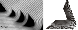
While it seems trivial due to its atomically thin structure controlled etch of 2D materials is critical to achieve sophisticated device structures such as LEDs, tunnel transistors or for side contacts to 2D materials. The relatively mature etch technology can therefore be easily tuned to etch stacks of these layers with profiles dictated by the device architecture. At the limit of controlled etching is the emerging field of Atomic Layer Etching (ALE). Significant advances in ALE methods of both conventional and 2D materials would enable further advances in atomic scale devices.
- Metrology and in-line quality control
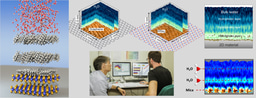
Important advances in the solutions of the above challenges requires non destructive characterization techniques both in-line and post fabrication. Techniques such as Raman spectroscopy and ThZ spectroscopy show great promise in providing significant insights into the structural and electronic properties. Correlation of material quality by evaluating device performance with spectral features obtained using these techniques would aid in standardization. This definition would enable scientists across the world to work towards the same goal and thereby further accelerate development of this exciting new technology.
Dr Ravi S Sundaram
Market Manager: Research and Emerging Technologies
Oxford Instruments Plasma Technology
North End, Yatton,
BS49 4AP

Please sign in or register for FREE
If you are a registered user on Research Communities by Springer Nature, please sign in