Atomic 3D nanofabrication enables reproducible atomic scale memristive switching
Published in Electrical & Electronic Engineering
Exascale computing is emerging due to the tremendous demand for the management of massive data resulting from everyday activities (mass storage medias, cell phones, internet of things etc). Yet, the current von Neumann computing architecture fundamentally produces an energetic bottleneck in particular when trying to manipulate, transmit, or process vast amount of data. This is because the power consumption per device does not scale down with the device dimension. As a consequence, disruptive technological platforms for making more efficient hardware’s implementations are definitely needed, especially, when device dimensions approach the single nanometer scale.
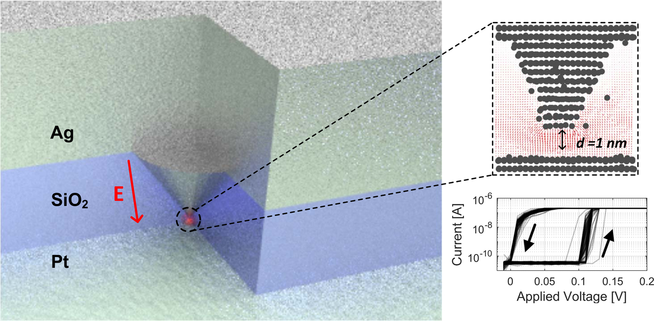
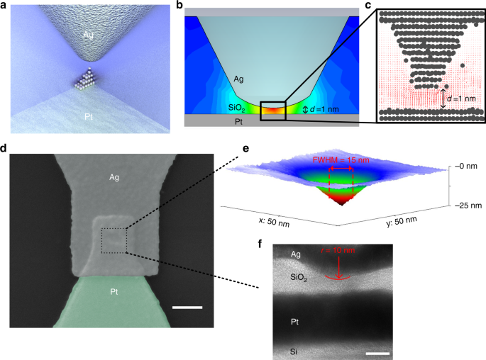
We achieved this by integrating an atomically sharp 3D tip into silica that reliably controls the relocation of single atoms within a 1 nm. At the nanometer scale, the shape of the atomic configuration plays an important role in the device performance and limits the reliability of devices. This is way we worked on a new fabrication technology to more precisely shape the atomic scale structure. As a concrete realization we present an Ag/SiO2/Pt electrochemical metallization cell, also known as conductive bridging random access memory (CBRAM) and show extraordinary results thanks to the novel fabrication platform that has been put in place.
In our research, we find that the higher the field confinement, the better the control of filament formation, the lower the switching voltage and the lower the cycle-to-cycle and cell-to-cell variance. For a 1nm device, we have achieved ultra low voltage of 100 mV, ultra-fast speed operation of 7 ns, excellent reliability and reproducibility.
In addition to the atomistic study, we implement ab-initio quantum transport simulation of the system. We found that the manufactured structures exhibit reduced self-heating effects due to their lower dimensions, making them very promising candidates to overcome the ever increasing power density challenge. The fabricated device has a nanometer footprint and the reduced self-heating facilitates high-density cross-bar integration situation.
It should be emphasized that the demonstrated fabrication platform is compatible with other memristive material systems and field confinement is certainly beneficial to other memristive switching schemes such as phase change material or valence change material.
Communications Physics (2019), DOI: 10.1038/s42005-019-0125-9
Follow the Topic
-
Communications Physics

An open access journal from Nature Portfolio publishing high-quality research, reviews and commentary in all areas of the physical sciences.
Related Collections
With Collections, you can get published faster and increase your visibility.
Physics-Informed Machine Learning
Publishing Model: Hybrid
Deadline: May 31, 2026
Advances in Quantum Networking: QKD and beyond
Publishing Model: Open Access
Deadline: Apr 30, 2026

Please sign in or register for FREE
If you are a registered user on Research Communities by Springer Nature, please sign in