Carbon nanotubes for flexible hybrid electronics
Published in Electrical & Electronic Engineering

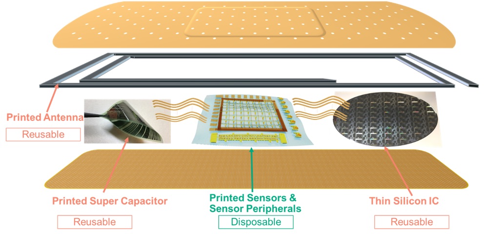
This work brings closer to the reality of an ultra-thin patch, highly conformable to skin surfaces, for accurately monitoring and analyzing the vital signs. The solution, based on flexible hybrid electronics (FHE), seamlessly integrates two technologies: low-cost, light-weight, and stretchable electronics by printing, and thinned silicon chips that are bonded to the same flexible substrate with printed electronics. An FHE patch, illustrated in Figure 1, offers greater comfort (wear-and-forget), enables continuous and non-invasive health monitoring, and could possibly be disposable once it reaches the economy of scale. However, before it is ready for the prime time, there are still a number of challenges to overcome in material development, circuit design and system integration.

Figure 1. A conceptual diagram of an FHE patch that includes printed sensors, sensor peripheral circuits, printed supercapacitors, printed antennas and thinned silicon chips.
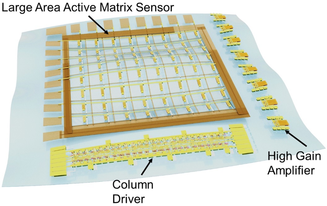
A thin FHE patch consists of several key components, including flexible sensors, flexible peripheral circuits, and the thin silicon chip. This study mainly addresses challenges in circuit design and fabrication for flexible sensor peripheral circuits which include sensor arrays, flexible column drivers and near sensor flexible amplifiers, as illustrated in Figure 2. Our solution is based on a solution-processed carbon nanotube (CNT) thin-film transistor (TFT), which we believe is a viable candidate for flexible and wearable electronics because of its high charge carrier mobility, high mechanical flexibility and good solution processability.

Figure 2. A 2-D flexible sensor array integrated with flexible column drivers and near sensor flexible amplifiers.
The key challenges of implementing CNT-TFT-based peripheral circuitry include the low semiconducting CNT purity (typically <99.9%), its correspondingly low device yield, and the mismatch between p- and n-type TFTs for short channel lengths to meet the circuit design needs. To realize complementary high-performance CNT circuits on flexible substrates, unstable n-type dopants and low-work-function metals are required, which inevitably increases fabrication complexity and therefore decreases the yield of complementary CNT circuits. In addition to low circuit yield, the inferior carrier mobility of n-type CNT TFTs and the mismatch of the threshold voltages between n- and p-type CNT TFTs often lead to sub-optimal circuit performance and circuit scaling, as well as higher power consumption.
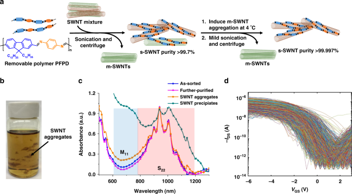
To address these challenges, in this study, we developed a novel sorting method that can achieve high purity (99.997%) and high yield (19.9%) separation of semiconducting CNTs. Systematic device fabrication and optimization for CNT deposition, dielectric/semiconductor interface, device configuration, and encapsulations lead to a much higher device yield, greater uniformity, and much better bias stability. Also, Pseudo-CMOS, for which only mono-type (ex. n- or p-type only) TFTs are used for logic implementation, is adopted to replace complementary logic which completely eliminate the dependency on any n-type CNT TFTs for circuit implementation.
With the joint efforts in device optimization and Pseudo-CMOS-based circuit design, we demonstrated high-performance 5-stage based ring oscillators running at up to 3.5 MHz, using only 2-µm p-type CNT TFTs. The benefits of using only high-performance p-type CNT TFTs are prominent in the circuit implementations of an 8-stage shift register consisting of 304 CNT TFTs operating at 50 kHz clock rate, as well as a tunable-gain amplifier with >1,000X voltage gain at 20 kHz. These circuits are foundational building blocks for implementing flexible sensor arrays (Figure 2) and flexible displays. The higher speed these circuits can achieve, the more and the broader applications these circuits can be used for. Our results show that bottom-contact device configuration and p-type only pseudo-CMOS design is a promising device-circuit solution to realizing circuits with greater performance than complementary-design-based circuits, in addition to its simpler process complexity which can enable large-scale flexible circuits. In summary, the combined effects of high CNT purity, TFT uniformity, and robust pseudo-CMOS design demonstrated in this study lead to flexible circuit implementation with unprecedented high yield, great scale, and the state-of-the-art performance.
The full study is available at Nat. Commun. 2019, 10, 2161.
Follow the Topic
-
Nature Communications

An open access, multidisciplinary journal dedicated to publishing high-quality research in all areas of the biological, health, physical, chemical and Earth sciences.
Related Collections
With Collections, you can get published faster and increase your visibility.
Women's Health
Publishing Model: Hybrid
Deadline: Ongoing
Biosensing
Publishing Model: Hybrid
Deadline: Jun 30, 2026


Please sign in or register for FREE
If you are a registered user on Research Communities by Springer Nature, please sign in