Giant Stark splitting of an exciton in bilayer MoS2
Published in Electrical & Electronic Engineering

Atomically thin transition metal dichalcogenides (TMDs), such a MoS2 and WSe2, strongly interact with light. Their optical properties are governed by excitons, electrons and holes bound by Coulomb attraction, that remain stable at room temperature. The ability to additionally tune their transition energies is essential for various interesting opto-electronic applications. This can in principle be achieved via the quantum-confined Stark effect by applying an electric field perpendicular to the sample plane.
In a single-layer MoS2, absorption can reach up to 100 %, but the optical transitions cannot be tuned in energy in devices with electrodes. Here, the carriers are confined to one single layer – these excitons have essentially no out-of-plane electric dipole. This demands to introduce a certain vertical distance between the electron and hole, forming electric dipole along the applied electric field direction.
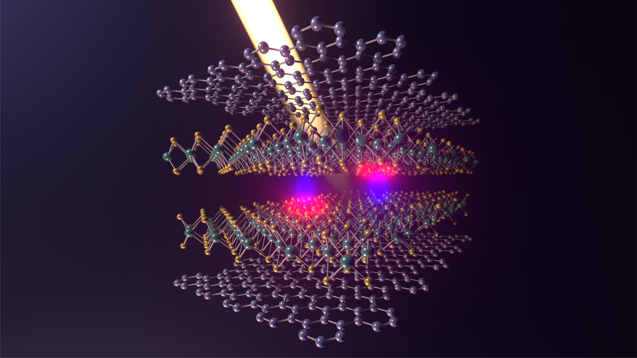
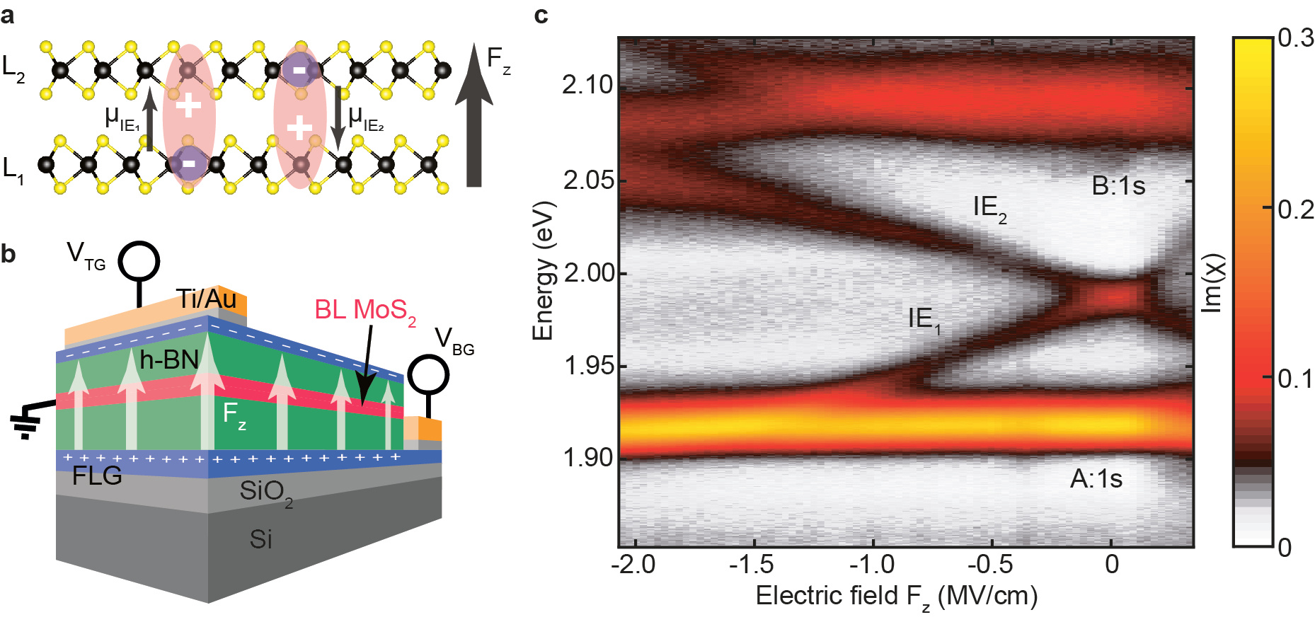
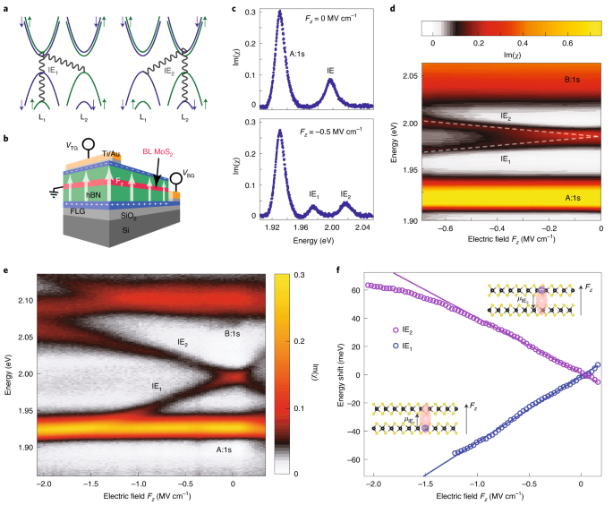
Experiments at the University of Basel and at LPCNO Toulouse, supported by beyond DFT calculations, have now uncovered optical transitions with strong absorption and wide tunability in the visible range of the optical spectrum in MoS2 bilayers. The main idea is to use transitions based on electrons and holes that do not reside in the same but in different layers, so called interlayer excitons. The separation between the electrons and the holes gives rise to a static electric dipole (Fig. a), and allows therefore tuning these transitions in applied electric fields. For practical device integration the researchers in Basel and Toulouse use atomically thin electrodes based on few-layer graphene (Fig. b). To find out which transition is tunable and which transition is not, careful comparison between the theoretically predicted localization of the carriers (in one of the layers, L1 or L2, or delocalized over both layers) and the experiments in applied magnetic and electric fields was crucial.

Figure: MoS2 bilayer van der Waals heterostructure (vdWH) in an applied electric field. a, Schematics of the interlayer excitons in homobolayer MoS2. An electron localized in one layer (L1 or L2) interacts with a hybridized hole state to form an interlayer exciton. b, Three-dimensional schematic of the device structure. c, Colour map of the optical absorption spectra as a function of the applied electric field.
The existence of an in-built dipole makes interlayer excitons not only tunable, but also introduces interactions between them (strong dipole-dipole interactions) (Fig. c). In the future it will be interesting to couple these excitons to optical microcavity modes (as recently demonstrated for III-V semiconductors in Nat. Mater. 18, 213–218 (2019)., Nat. Mater. 18, 219–222 (2019).), where strong interactions between the particles are needed to work towards single polariton switches.
This work was recently published in Nature Nanotechnology:
Giant Stark splitting of an exciton in bilayer MoS2
Nadine Leisgang, Shivangi Shree, Ioannis Paradisanos, Lukas Sponfeldner, Cedric Robert, Delphine Lagarde, Andrea Balocchi, Kenji Watanabe, Takashi Taniguchi, Xavier Marie, Richard J. Warburton, Iann C. Gerber, and Bernhard Urbaszek
Nature Nanotechnology (2020), https://www.nature.com/articles/s41565-020-0750-1
Follow the Topic
-
Nature Nanotechnology

An interdisciplinary journal that publishes papers of the highest quality and significance in all areas of nanoscience and nanotechnology.


Please sign in or register for FREE
If you are a registered user on Research Communities by Springer Nature, please sign in