Looking Beyond Surface Area: How Disorder Helped Us Detect Invisible Pollutants






A Hidden Challenge in Persistent Pollutants
Our motivation arose from a pressing environmental challenge. Many pollutants released into soil and water, including chlorinated pesticides, polycyclic aromatic hydrocarbons and fluorinated microplastics, are highly resistant to degradation. As a result, they can persist for decades and pose long-term risks to ecosystems and human health (Figure 1a).
Detecting these pollutants at trace concentrations is therefore essential. Surface-enhanced Raman spectroscopy (SERS) is a powerful tool for trace detection, but traditional gold or silver substrates often fail to capture these weakly interacting molecules (Figure 1b). This led us to a fundamental question: could we design a more effective semiconductor-based SERS material?
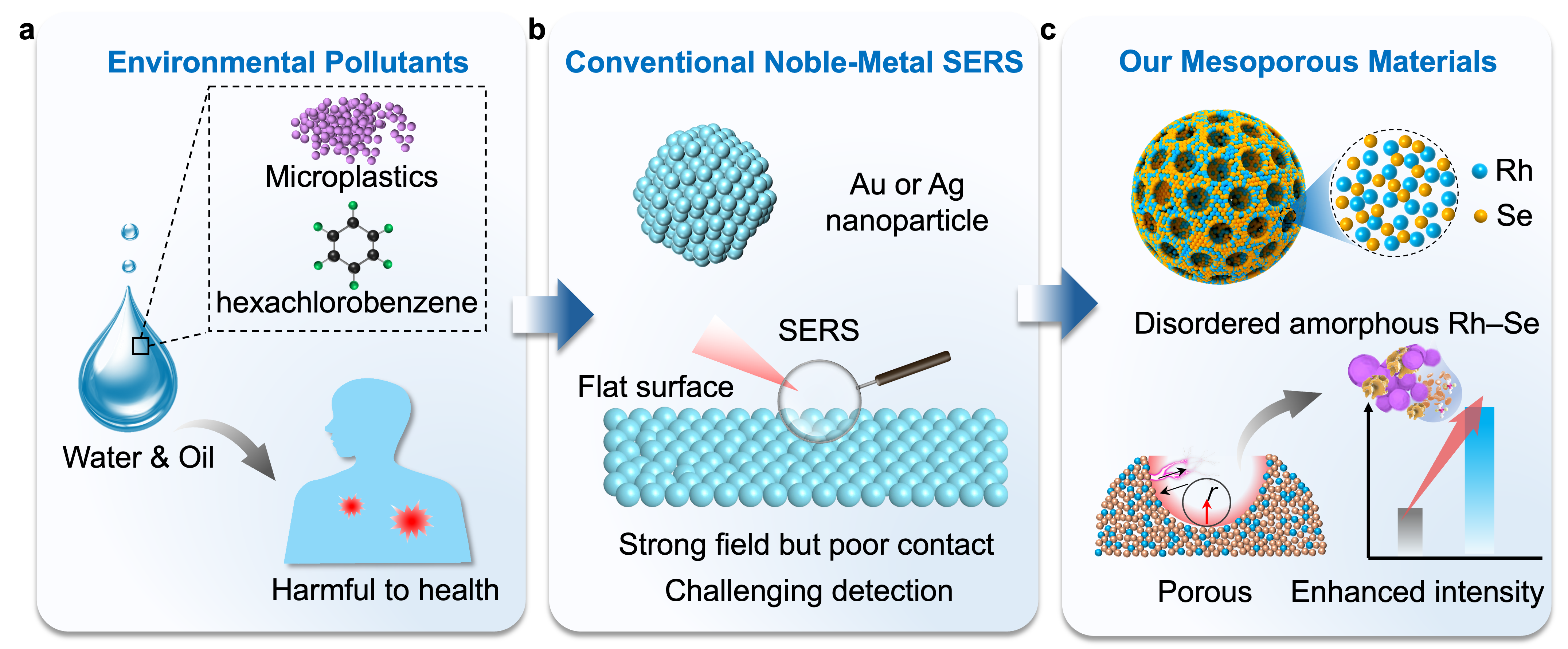
Figure 1. New material for detecting environmental pollutants. (a) Environmental pollutants like microplastics and hexachlorobenzene are found in water and oil sources, posing significant health risks. (b) Conventional surface-enhanced Raman spectroscopy (SERS) methods, shown in the center panel, utilize Au or Ag nanoparticles on a flat surface. While they create strong electromagnetic fields, they suffer from poor contact with large or irregularly shaped pollutants, making detection challenging. (c) Our novel mesoporous material consists of disordered, amorphous Rh-Se. This unique porous structure allows for better encapsulation and concentration of pollutants within the material, leading to a greatly enhanced SERS intensity and significantly improved detection capabilities.
Building a Material That Was Difficult to Make
We focused on amorphous rhodium selenide (Rh–Se), a material that combines metallic and semiconducting characteristics (Figure 1c). Its disordered atomic structure offers unique electronic properties that are difficult to achieve in crystalline materials.
Synthesizing amorphous Rh–Se, however, was highly challenging. Rh readily crystallizes, and maintaining both an amorphous framework and an ordered mesoporous structure required precise control over precursor ratios, reaction conditions, templates, and reduction kinetics. Small changes often led to collapsed pores or unwanted crystalline phases.
After extensive optimization, we developed a one-step micellar self-assembly strategy that enabled the synthesis of highly amorphous Rh–Se mesoporous nanospheres with tunable pore sizes.
When the Data Challenged the Textbook View
To understand how the material worked, we systematically varied two structural parameters. The first was surface curvature, which we tuned by changing pore size (Figure 2a). The second was crystallinity, which we adjusted through thermal annealing.
Our initial expectation seemed straightforward. Smaller pores should provide larger surface areas and more adsorption sites. According to conventional SERS design principles, these samples should have produced the strongest signals.
However, the experiments showed the opposite.
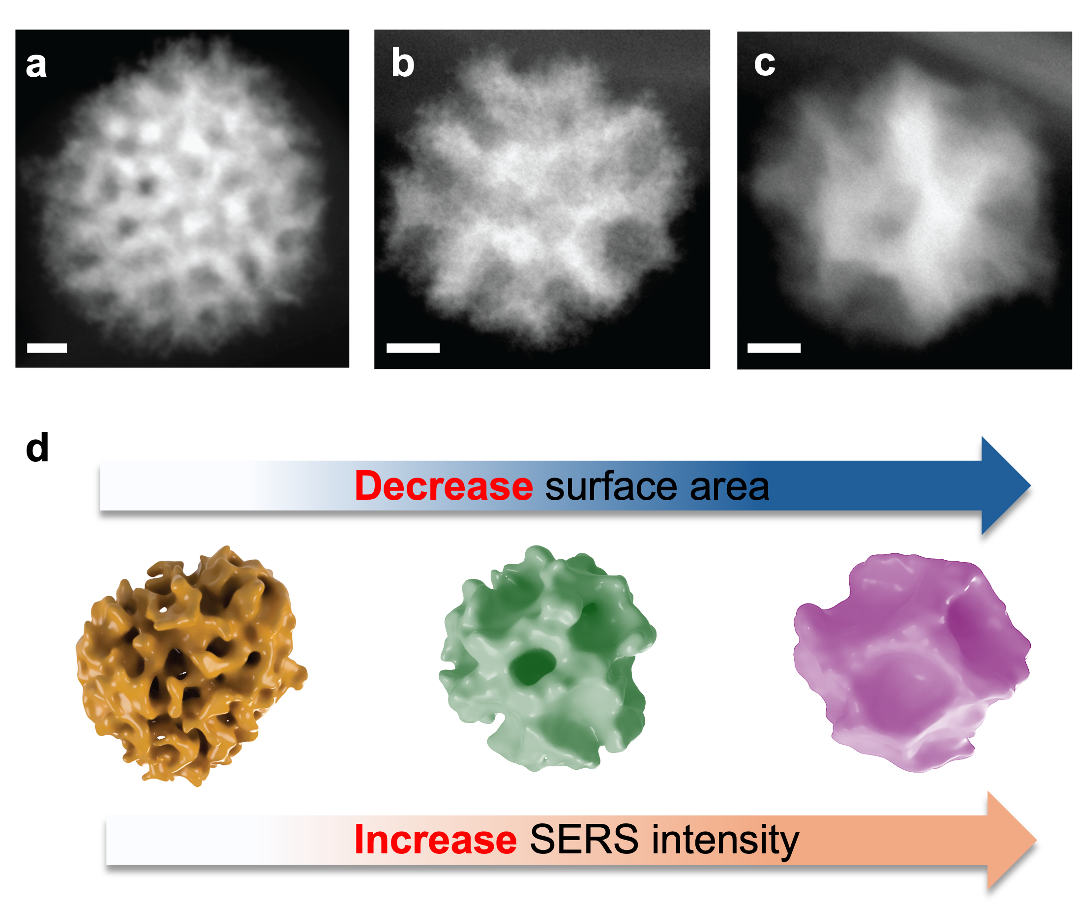
Figure 2. Structural characterization and SERS performance of Rh-Se nanostructures with tunable pore sizes. (a–c) Representative transmission electron microscopy images of Rh-Se nanostructures with increasing pore dimensions. Scale bars: 20 nm. (d) Schematic illustration showing the correlation between pore structure, surface area, and SERS intensity. As the pore size increases, the specific surface area decreases, but leading to an enhancement in SERS intensity.
Samples with the largest pores, despite having the lowest surface area, consistently produced the strongest Raman enhancement (Figure 2b).
Our first response was disbelief. We repeated the synthesis several times, checked the Raman measurements carefully, and re-examined the morphology, composition, pore structure, and electronic properties using multiple characterization techniques.
Each experiment confirmed the same trend. The result was real.
Looking Beyond Surface Area
Once we accepted the observation, the more important question emerged: why did larger pores perform better?
The answer gradually came from spectroscopy, microscopy, atomic force microscopy, synchrotron X-ray characterization, and theoretical calculations carried out with collaborators across several countries.
Larger pores did not simply change the number of adsorption sites. Instead, they subtly altered the electronic structure of the amorphous Rh–Se framework. At the same time, the disordered atomic arrangement created abundant electronically active sites.
Together, these structural features lowered the energy barrier for charge transfer between the semiconductor and pollutant molecules.
In other words, sensing performance was governed less by the amount of surface area available and more by how efficiently electrons moved across the substrate-analyte interface.
This finding challenges a common assumption in semiconductor SERS design. Rather than maximizing surface area alone, tuning electronic structure through curvature engineering and amorphization may offer a more effective strategy.
Detecting Real Pollutants, Not Only Model Molecules
Another rewarding aspect of this work was moving beyond the model molecules commonly used in laboratory SERS studies.
Many published demonstrations rely on dyes that readily adsorb onto sensing surfaces and generate strong Raman signals. Real environmental pollutants are far less cooperative.
We therefore tested our materials against several chemically resistant pollutants, including hexachlorobenzene, anthracene and PTFE microplastics suspended in wastewater. These molecules are difficult to detect because they interact weakly with conventional semiconductor surfaces.
Seeing clear Raman fingerprints from such challenging samples was one of the most exciting moments of the project. It suggested that the design principles uncovered here could extend beyond one material system.
More broadly, this work points to a route for developing semiconductor sensing platforms for real environmental monitoring.
Learning from Unexpected Results
Looking back, perhaps the most valuable lesson from this project is not about Rh, Se or even SERS itself.
Scientific progress often begins when experiments refuse to behave as expected. If we had dismissed our measurements because they contradicted the assumption that higher surface area always improves performance, we might have missed the underlying mechanism.
Instead, the unexpected observation forced us to rethink how material structure shapes electronic behaviour.
We hope this work encourages researchers to look beyond conventional design rules and pay close attention to surprising results. Sometimes the most important discoveries are not found in experiments that confirm our expectations, but in those that challenge them.
Those moments of curiosity are often where science moves forward.

Follow the Topic
-
Nature Communications
An open access, multidisciplinary journal dedicated to publishing high-quality research in all areas of the biological, health, physical, chemical and Earth sciences.

Related Collections
With Collections, you can get published faster and increase your visibility.
Women's Health
Publishing Model: Hybrid
Deadline: Ongoing
Tumor Microenvironment Crosstalk and Therapeutic Implications
Publishing Model: Hybrid
Deadline: Nov 02, 2026