Monolithic Integration of Redox-Stable Sn–Pb Halide Perovskite Single-Crystalline Films for Durable Near-Infrared Photodetection
Published in Materials

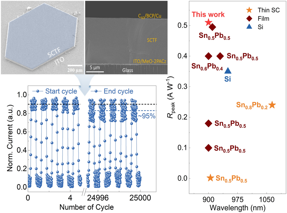
Tin–lead (Sn–Pb) halide perovskite single crystals combine narrow bandgaps, long carrier diffusion lengths, and low trap densities, positioning them as ideal candidates for near-infrared (NIR) optoelectronics. However, conventional growth strategies rely on bulk crystallization at elevated temperatures, leading to uncontrolled nucleation, Sn2+ oxidation, and poor compatibility with planar integration. Here, we develop a coordination-engineered crystallization strategy that enables direct, low-temperature growth of micrometer-thick Sn–Pb single-crystal thin films on device-compatible substrates. By modulating metal–solvent coordination strength using a low-donor number cosolvent system, we delineate a narrow processing window that stabilizes precursor speciation, lowers the nucleation barrier, and guides directional crystal growth under mild thermal conditions (< 40 °C). The resulting crystal films exhibit smooth morphology, high crystallinity, compositional uniformity, and ultralow trap densities (~ 3.98 × 1012 cm−3). When integrated into NIR photodetectors, these films deliver high responsivity (0.51 A W−1 at 900 nm), specific detectivity up to 3.6 × 10¹² Jones, fast response (~ 188 μs), and > 25,000 cycles of ambient operational stability. This approach establishes a scalable platform for redox-stable, low-temperature growth of Sn–Pb perovskite crystal films and expands the processing–structure–function landscape for next-generation infrared optoelectronics.
Editor of Nano-Micro Letters, which is an Open-Access, peer-reviewed journal reported papers that have at least one dimension ranging from a few sub-nanometers to a few hundreds of micrometers. The journal is published by Springer Nature and indexed by SCI, EI, SCOPUS, Pubmed, etc. The 2025 JCR Impact Factor is 38.5. The 2025 CiteScore is 58.9.
Follow the Topic
-
Nano-Micro Letters
Nano-Micro Letters is a peer-reviewed, international, interdisciplinary and open-access journal that focus on science, experiments, engineering, technologies and applications of nano- or microscale structure and system in physics, chemistry, biology, material science, and pharmacy.


Please sign in or register for FREE
If you are a registered user on Research Communities by Springer Nature, please sign in