Room-temperature direct synthesis of semiconductive PbS nanocrystal inks for optoelectronic applications
Published in Electrical & Electronic Engineering
Lead chalcogenide nanocrystals (NCs) are promising materials with high bandgap-tunability for flexible and lightweight infrared optoelectronics, which is also compatible with low-cost, large-scale manufacturing on plastic substrates.
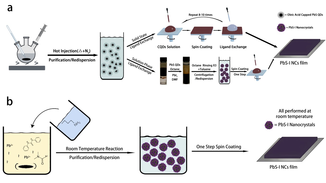
Currently, ligand exchange is essential for NCs based optoelectronics, which can replace insulating long-chain-ligands with shorter ones to increase carrier mobility. However, the ligand exchange process is normally tedious, extravagant and can be only implemented with lab-scale, which hinders the commercial possibility of NC based optoelectronics (Figure 1a). Apparently, the existence of long organic-ligand is impeditive for the final optoelectronic applications. If the semi-conducting NCs ink can be synthesized directly, it will definitely largely reduce manufacturing costs and promote the industrial application of NCs.
In this work, we developed a new method to direct synthesize halide capped semi-conducting metal chalcogenide NC inks for optoelectronic applications. Metal halide and N, N-Diphenyl thiourea (DPhTA) are employed as precursors. Based on this method, in situ halide capped PbS, Ag2S and CdS NC inks are directly synthesized at room temperature, showing excellent scalability and versatility (Figure 1b). We have also demonstrated a lab scale-up synthesis to increase the reaction volume to 2 L and obtained more than 88 g PbS NC ink solids in one pot, with the cost of PbS NC inks lower than 6 $/g. Furthermore, Obtained PbS NC inks show good size tunability and state-of-the-art performance for optoelectronic applications. Based on these PbS NC inks, photodetectors show a high detectivity up to 1.4 × 10^11 Jones at 635 nm with a fast response time less than 4 ms and photovoltaic devices show a power conversion efficiency (PCE) up to 10% with superior device air stability, which outperform the control devices based on solution-phase ligand exchanged NCs.
Our results may pave a path for the future commercialization of NC based optoelectronics.

Figure 1. Schematic representation of different preparations for PbS-I NC films. (a) Conventional two-step “synthesis to ligand-exchange” process and (b) our one step direct synthesis of iodide capped PbS NCs inks.
These results were recently published in Nature Communications:
https://www.nature.com/articles/s41467-019-13158-6
Follow the Topic
-
Nature Communications
An open access, multidisciplinary journal dedicated to publishing high-quality research in all areas of the biological, health, physical, chemical and Earth sciences.

Related Collections
With Collections, you can get published faster and increase your visibility.
Women's Health
Publishing Model: Hybrid
Deadline: Ongoing
Biosensing
Publishing Model: Hybrid
Deadline: Sep 30, 2026


Please sign in or register for FREE
If you are a registered user on Research Communities by Springer Nature, please sign in