Van der Waals assembly brings functional 3D crystalline Lego bricks to established integrated photonic platforms

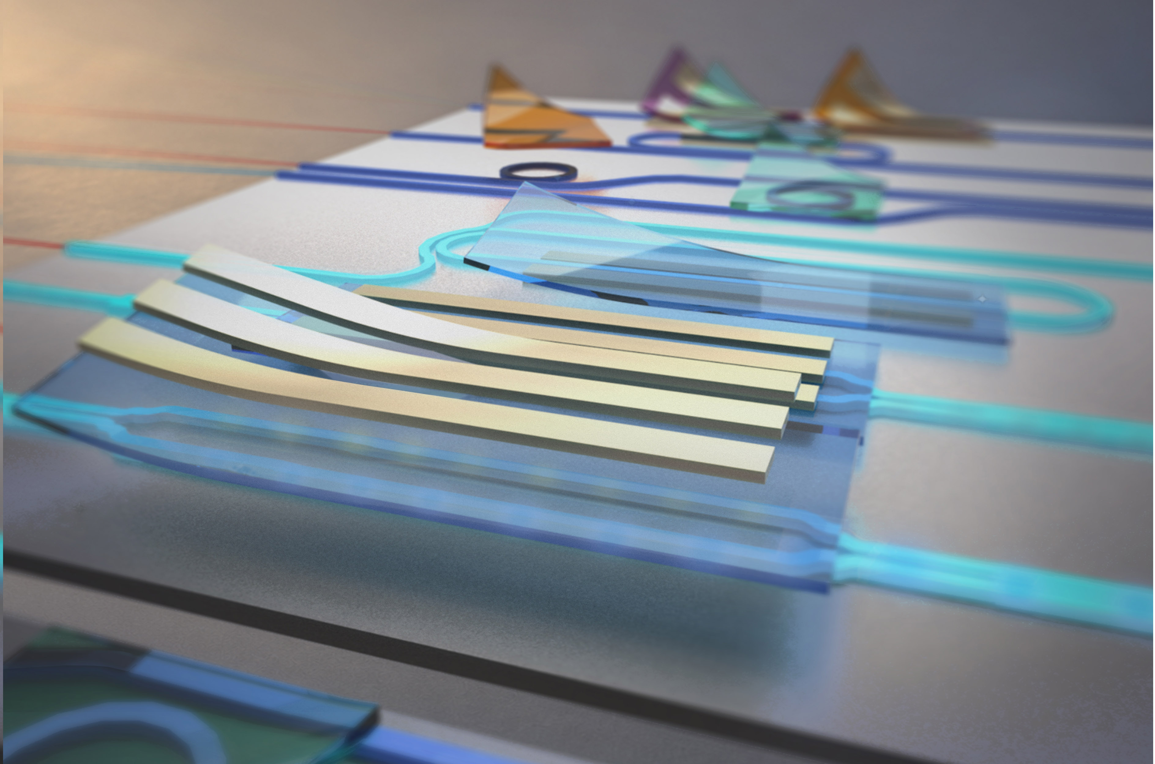

A new assembly rule for heterogeneous photonics
Modern photonic circuits are usually built around silicon or silicon nitride because these platforms guide light efficiently and support advanced nanofabrication. Yet the materials that most effectively modulate light, break optical reciprocity or absorb particular wavelengths often belong to entirely different crystal families. Bringing those functions onto one chip has remained difficult because conventional crystal growth couples two decisions that ideally should be independent: the substrate needed to grow a high-quality film and the substrate needed to guide and process light.
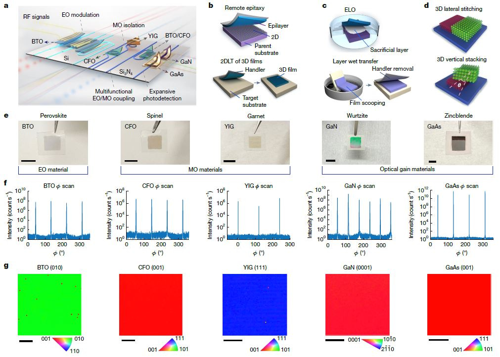
Our recent Nature study now demonstrates a viable solution to separate those decisions [1]. Instead of forcing a functional crystal to grow directly on Si or SiN with non-ideal quality, we grow it on a parent substrate chosen for its crystal chemistry, release it as an ultrathin single crystal, and then assemble it on a completed photonic circuit. Interfacial adhesion enables integration without requiring continuous chemical bonding or lattice registry across the receiving interface. The functional layer therefore arrives on the chip with the crystallinity—and, critically, the crystallographic orientation—needed for its optical response.
From naturally layered materials to transferable 3D crystals
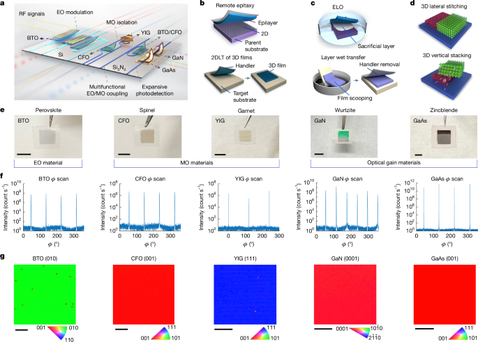
Van der Waals heterostructures are best known as stacks of naturally layered two-dimensional (2D) materials. The present work generalizes that design logic to non-layered, three-dimensional crystals [2, 3]. Epitaxial lift-off and 2D-material-assisted layer transfer were used to prepare freestanding nanomembranes of BTO, CFO, YIG, GaAs and GaN [4, 5]. These materials represent crystal structures and functions that cannot normally be combined through a single heteroepitaxial growth sequence (Figure 1).
Once detached, the membranes become modular photonic building blocks. They can be rotated to align an anisotropic tensor with a waveguide field, placed side by side to allocate different spectral tasks to different semiconductors, or stacked to bring electric and magnetic control into the same optical structure. This physical-assembly approach is the paper’s broader conceptual contribution: it treats material identity, crystal orientation and three-dimensional placement as selectable elements of photonic design.
Efficient EO modulation by vdW-integrated single-crystalline BTO nanomembranes
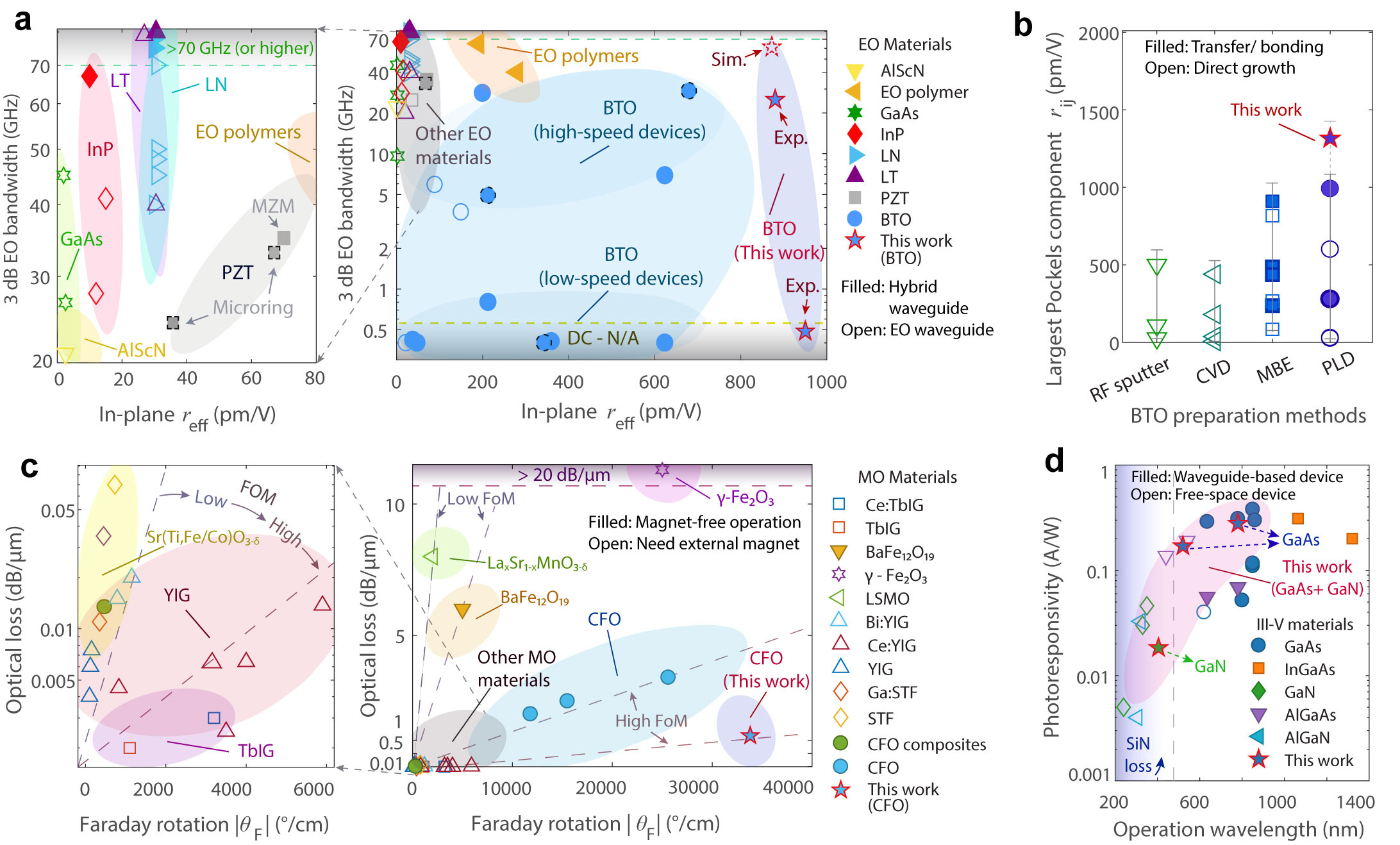
BTO can possess a much stronger Pockels effect than widely used integrated electro-optic (EO) crystals, but only if its domain state and crystal axes are correctly coupled to the electric and optical fields [6-9]. The team transferred predominantly a-axis-domain BTO onto Si and aligned the membrane at approximately 45° to the waveguide. A Mach–Zehnder modulator then reached VπL ≈ 0.29 V·cm (DC/low frequency), with an effective in-plane Pockels coefficient of approximately 950 pm/V and an inferred r42 around 1,290 pm/V.
A separately engineered travelling-wave device addressed high-speed operation. With a thinner BTO layer, an SiO₂ spacer and microwave electrodes designed for impedance and velocity matching, it achieved a 3-dB EO bandwidth above 23 GHz (VπL ~1.4 V·cm at 2 MHz), with the extracted effective Pockels coefficient was ~880 pm/V. Together, these devices establish both the intrinsic efficiency made accessible by crystallographic control and the compatibility of the transferred crystal with high-speed photonic design; the headline efficiency and bandwidth values arise from different optimized modulators.
Magneto-optical insolation and wide-band on-chip photodetection
In the magnetic branch of the study, CFO provided a large magneto-optic response on a Si microring. The ring exhibited direction-dependent resonance splitting and more than 18 dB extinction under an applied magnetic field. From the measured response, we extracted a Faraday rotation coefficient of approximately 33,800°/cm. The hard-magnetic CFO also retained its magnetization after the field was removed, supporting nonreciprocal operation after magnetization without a continuously applied external magnet.
Freestanding GaAs and GaN nanomembranes were also vdW-integrated on the same SiN circuit for photodetection. GaAs detected 780-nm and 520-nm light with responsivities of 0.29 and 0.16 A/W, respectively, while GaN detected 405-nm light with a responsivity ~17 mA/W. The devices are proof-of-concept demonstrations at discrete wavelengths, but they show how a photonic circuit can acquire a tailored spectral response by assigning each wavelength range to a semiconductor with an appropriate bandgap.
We also combined electric and magnetic functionality vertically. A CFO/SiO2/BTO stack was assembled on one Si microring, yielding electro-optic tuning from BTO and magneto-optic nonreciprocity from CFO in the same device structure. Such a stack created an artificial 3D heterostructure in which distinct single-crystalline responses can interact with the same resonator and, with further design, potentially the same optical mode.
Outlook for vdW-integration-based heterogeneous photonic integration
The work shifts the materials question from "growing desired functional layers directly on photonic chip with compromised quality" to " selecting which freestanding single-crystalline building blocks to be released and positioned on arbitrary established photonic platform" with unrivalled performances (Figure 2). That change is consequential for platforms whose best functional materials demand mutually incompatible growth substrates or thermal budgets (Figure 3). It also creates experimental access to combinations of ferroelectric, magnetic and semiconducting crystals that could support coupled phenomena, hybrid-dimensional moiré structures and topological photonic architectures [3, 10-12].
The reported process spans laboratory-scale membranes and a one-inch-diameter BTO transfer. Microscopy and optical measurements show smooth surfaces, sharp interfaces and strong bonding, with thermal treatment converting the initial van der Waals gap into a robust interface. Scaling the concept into a manufacturing technology will require automated transfer and alignment, wafer-level uniformity, high yield, process-design rules and reliability data [13, 14]. The present contribution is the experimentally validated foundation: disparate functional 3D single crystals can be synthesized under their preferred conditions and subsequently composed on mature photonic circuits without surrendering the material quality on which device performance depends for advanced heterogeneous integrated photonics [15, 16].

Article Information
Heterogeneous van der Waals integration of single-crystalline photonic nanomembranes, Nature (2026).
DOI: 10.1038/s41586-026-11000-w
Authors includes Dr. Yuan Meng, Dr. Wenbo Mao, Mr. Zhihao Xu, Dr. Di Jia, and contributions from Qian Zhang, Weijie Xu, Mingfeng Chen, et al. from Washington University in St. Louis (WUSTL), Mengxin Lin and Jianqi Hu from EPFL, Jisung Seo and Bora Kim from UIUC, Xinyuan Zhang and other collaborators from MIT. Prof. Sang-Hoon Bae and prof. Lan Yang (WUSTL) supervised the project, as well as supports from prof. Tobias J. Kippenberg (EPFL), prof. Hyunseok Kim and prof. Minjoo Larry Lee (UIUC), prof. Frances M. Ross and prof. Jeehwan Kim (MIT), prof. Cheng-Wei Qiu (NUS), and prof. Sheng Ran and prof. Xi Wang (WUSTL), et al. from multiple universities.
We also sincerely thank ECCI measurement assistance from Dr. Seong Ho Cho at Massachusetts Institute of Technology (MIT), FIB assistance from Dr. Huafang Li at Washington University in St. Lous (WUSTL), and helpful discussions from Dr. Sangho Lee at MIT and Dr. Edwin Carlen at WUSTL, and the cleanroom facilities support from IMSE at WUSTL, HMNTL at UIUC, and MTL at MIT.
Article link
https://www.nature.com/articles/s41586-026-11000-w
References
[1] Y. Meng et al. “Heterogeneous van der Waals integration of single-crystalline photonic nanomembranes.” Nature (2026).
[2] Y. Liu et al. “Van der Waals integration before and beyond two-dimensional materials.” Nature 567, 323–333 (2019).
[3] Y. Meng et al. “Photonic van der Waals integration from 2D materials to 3D nanomembranes.” Nature Reviews Materials 8, 498–517 (2023).
[4] H. Kum et al. “Epitaxial growth and layer-transfer techniques for heterogeneous integration of materials for electronic and photonic devices.” Nature Electronics 2, 439–450 (2019).
[5] H. Kim, et al. "Remote epitaxy." Nature Reviews Methods Primers 2, 40 (2022).
[6] S. Abel, et al. "Large Pockels effect in micro- and nanostructured barium titanate integrated on silicon." Nature Materials 18, 42–47 (2019).
[7] D. Chelladurai, et al. "Barium titanate and lithium niobate permittivity and Pockels coefficients from megahertz to sub-terahertz frequencies." Nature Materials 24, 868–875 (2025).
[8] C. Wang, et al. “Lithium tantalate photonic integrated circuits for volume manufacturing.” Nature 629, 784–790 (2024).
[9] H. Feng, et al. "Integrated lithium niobate microwave photonic processing engine." Nature 627, 80–87 (2024).
[10] G. Sánchez-Santolino, et al. “A 2D ferroelectric vortex pattern in twisted BaTiO3 freestanding layers.” Nature 626, 529–534 (2024).
[11] H. Tang, et al. "An adaptive moiré sensor for spectro-polarimetric hyperimaging." Nature Photonics 19, 463–470 (2025).
[12] M. Chen, et al. "Bichromatic moiré superlattices for tunable quadrupolar trions and correlated states." Nature Communications 16, 10359 (2025).
[13] Y. Meng, et al. "Functionalizing nanophotonic structures with 2D van der Waals materials." Nanoscale Horizons 8, 1345-1365 (2023).
[14] H. Xu, et al. "Two-dimensional materials for integrated sensing." Nature Materials (2026).
[15] Z. Qiu, et al. "High-pulse-energy integrated mode-locked laser using a Mamyshev oscillator." Nature 654, 57–63 (2026).
[16] Z. Tao, et al. "Ultrabroadband on-chip photonics for full-spectrum wireless communications." Nature 645, 80–87 (2025).
Follow the Topic
-
Nature
A weekly international journal publishing the finest peer-reviewed research in all fields of science and technology on the basis of its originality, importance, interdisciplinary interest, timeliness, accessibility, elegance and surprising conclusions.

Related Collections
With Collections, you can get published faster and increase your visibility.
Carbon Dioxide Removal
Publishing Model: Hybrid
Deadline: Jan 16, 2027
Cancer Neuroscience: from mechanisms to therapy
Publishing Model: Hybrid
Deadline: Jan 30, 2027