Van der Waals heterojunctions of 2D organic–inorganic materials for high-performance photodetectors
Published in Bioengineering & Biotechnology, Materials, and Physics
Key Experimental Findings
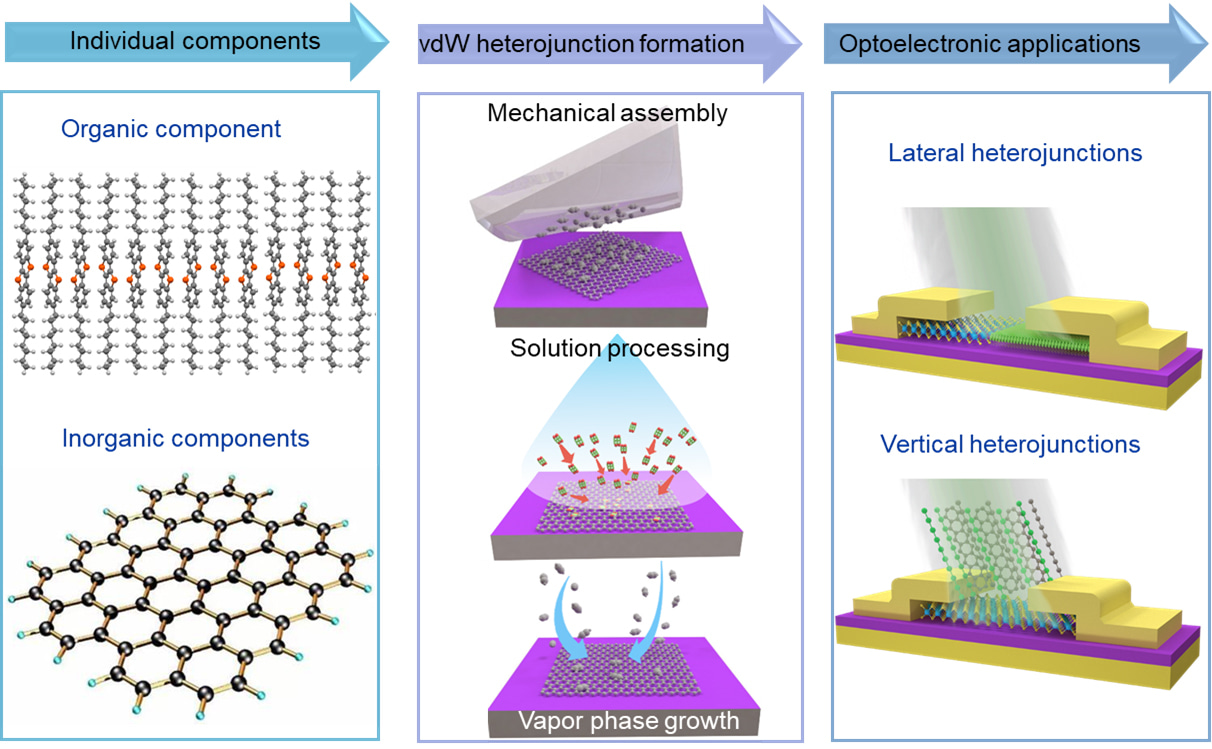
1. Versatile Fabrication
The review details diverse synthesis strategies, ranging from “bottom-up” approaches like physical vapor transport (PVT) for creating atomically ordered interfaces, to scalable “top-down” solution processing methods like spin coating and drop casting.
2. Superior Performance
Devices based on these vdWHs demonstrate exceptional metrics. For instance, phototransistors combining organic dyes with graphene have achieved responsivities exceeding 105 A/W, while others utilizing rubrene/graphene interfaces reached responsivities up to 107 A/W, significantly outperforming traditional devices.
3. Band Alignment Control
The study categorizes these heterojunctions into Type-I, Type-II, and Type-III band alignments. Type-II (staggered gap) configurations were found to be particularly effective for high-performance optoelectronics by promoting efficient electron-hole separation.
Mechanistic Insights
Synergistic Integration: the core advantage lies in the complementary nature of the components. Organic layers provide strong absorption coefficients and tunable bandgaps, while the inorganic 2D layers ensure rapid carrier transport.
Interface Quality: unlike conventional heterojunctions, vdWHs are formed via weak van der Waals forces without requiring strict lattice matching. This results in “dangling-bond-free” interfaces that minimize defect densities and charge traps, thereby enhancing carrier lifetime and transport efficiency.
Gating Effects: the review elucidates the role of the photogating effect (PGE) in these hybrid devices, where charged traps modulate channel conductivity, leading to high gain and sensitivity even under weak light conditions.
Technological Implications
This comprehensive overview paves the way for next-generation device applications:
Flexible Electronics: the mechanical flexibility of both 2D materials and organic thin films makes these vdWHs ideal for wearable technology and curved image sensors.
Broadband Detection: by selecting specific organic molecules, the spectral response of photodetectors can be tuned from ultraviolet to near-infrared, enabling versatile applications in optical communication and remote sensing.
Low-Cost Manufacturing: the compatibility of these materials with solution-based processing offers a pathway toward low-cost, large-area device fabrication compatible with varying substrates.
Challenges and Future Directions
While the potential is vast, several hurdles remain for commercial adoption:
1. Scalability: developing reliable techniques for the wafer-scale synthesis of uniform 2D organic-inorganic vdWHs remains a critical challenge, as current mechanical transfer methods are limited in size and yield.
2. Stability: the environmental sensitivity and lower thermal stability of organic components require advanced encapsulation and synthesis strategies to ensure long-term device durability.
3. Interface Optimization: future research must focus on balancing the trade-off between increasing the thickness of the organic layer for better absorption and maintaining efficient charge transport across the interface.
Conclusion
2D organic–inorganic vdWHs represent a paradigm shift in optoelectronics, offering a unique toolkit to design custom-tailored photodetectors. As fabrication techniques mature and stability issues are addressed, these hybrid materials are poised to drive the future of flexible, high-performance sensing technologies.
Follow the Topic
-
Moore and More
This is the first top-tier journal dedicated to Beyond Moore technology in the field of integrated circuit.


Please sign in or register for FREE
If you are a registered user on Research Communities by Springer Nature, please sign in