Vertical Interfacial Engineering in Two-Step-Processed Perovskite Films Enabled by Dual-Interface Modification for High-Efficiency p-i-n Solar Cells
Published in Bioengineering & Biotechnology and Materials
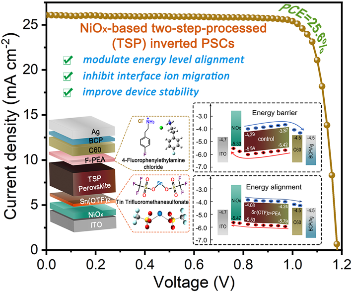
Two-step-processed (TSP) inverted p-i-n perovskite solar cells (PSCs) have demonstrated significant promise in tandem applications. However, the power conversion efficiency (PCE) of TSP p-i-n PSCs rarely exceeds 24%. Here, we demonstrate that TSP perovskite films exhibit a vertically gradient distribution of residual PbI2 clusters, which form Schottky heterojunctions with the perovskite, leading to substantial interfacial energy-level mismatches within NiOx-based TSP p-i-n PSCs. These limitations were effectively addressed via a vertical interfacial engineering enabled by dual-interface modification incorporating tin trifluoromethanesulfonate (Sn(OTF)2) and 4-Fluorophenylethylamine chloride (F-PEA) at the NiOx/perovskite and perovskite/C60 interfaces, respectively. The functional Sn(OTF)2 not only enhances the conductivity of NiOx films but also suppresses ion migration, while inducing the formation of a Pb-Sn mixed perovskite interlayer that precisely regulates the energy level at the NiOx/perovskite interface. Complementally, F-PEA post-treatment effectively converts surface residual PbI2 clusters into a 2D perovskite capping layer, which simultaneously passivates surface defects and enhances energy-level alignment at the perovskite/C60 interface. Consequently, the optimized NiOx-based TSP p-i-n PSCs achieve a notable PCE of 25.6% with superior operational stability. This study elucidates the underlying mechanisms limiting the efficiency of TSP p-i-n PSCs, while establishing design principles for these devices targeting 26% efficiency.
Editor of Nano-Micro Letters, which is an Open-Access, peer-reviewed journal reported papers that have at least one dimension ranging from a few sub-nanometers to a few hundreds of micrometers. The journal is published by Springer Nature and indexed by SCI, EI, SCOPUS, Pubmed, etc. The 2024 JCR Impact Factor is 36.3. The 2024 CiteScore is 53.1.
Follow the Topic
-
Nano-Micro Letters

Nano-Micro Letters is a peer-reviewed, international, interdisciplinary and open-access journal that focus on science, experiments, engineering, technologies and applications of nano- or microscale structure and system in physics, chemistry, biology, material science, and pharmacy.


Please sign in or register for FREE
If you are a registered user on Research Communities by Springer Nature, please sign in