A quantum touch of bismuth
Published in Materials

Background
It's over 40 years since the integer quantum Hall effect (QHE) and fraction quantum Hall effect (FQHE) were discovered in the two-dimensional electron gas in quantum wells .[1-2] To date, the known two-dimensional electron gas (2DEG) systems capable of realizing the QHE, especially the FQHE, still remain very limited. Recently, emerging 2D high mobility semiconducting materials have manifested great potential in not only fundamental physics but also nano-electronic applications. However, achieving the low-temperature fractional quantum Hall states in high-mobility intrinsic two-dimensional semiconductors through electrical transport has proven particularly challenging, with the main bottleneck being the difficulty of obtaining Ohmic contacts at relatively low carrier concentrations.
Historically, long after the FQH was found in high mobility electron gas in semiconductor quantum wells in the 1980s, graphene manifested its first set of FQH curves in the 2010s due to the experimental breakthrough of obtaining samples in the clean limit (either by suspending graphene, or by hexagonal boron nitride encapsulation), which drastically boosted its mobility. The unique SU(4) symmetry breaking of Landau levels (LLs) in graphene has enabled a new interaction regime, revealing even denominator FQH states in the lowest LL and in higher LLs. [3-5]
Different from graphene, transition metal dichalcogenides (TMDs) such as MoS2 has peculiar spin-valley degrees of freedom, a lot heavier effective masses (which is in favor of e-e interactions), and high intrinsic mobility, which offer the possibilities of spin manipulation for quantum information processing. As such, TMDs are the missing link between graphene and heterostructures such as GaAs. Recently, spectra of LLs in TMDs are intensively studied experimentally. Yet most of those studies are far above the quantum limit (i.e., only filling fractions ν > 1 are seen).[6-7] Quantized fractional quantum Hall plateaus in TMDs, especially at the lowest LLs where electron interactions are the most pronounced, has been missing so far, mainly due to two major challenges:
1. To reach the extreme quantum limit, one needs ohmic contact even at the low carrier density limit close to the band edge. So far, the several techniques developed (such as Pt bottom contact, phase engineering, and etc.[8]) to eliminate the Schottky barriers between the gapped TMDs and metal contacts are still far from being satisfactory at very low temperatures, which kills most of the chances of seeing the filling fraction of ν = 1 in the quantum Hall regime.
2. Except the electrical contact, dielectric screening conditions are also very important for obtaining the fractionally charged quantum excitations, which has been overlooked thus far.
Experimental results
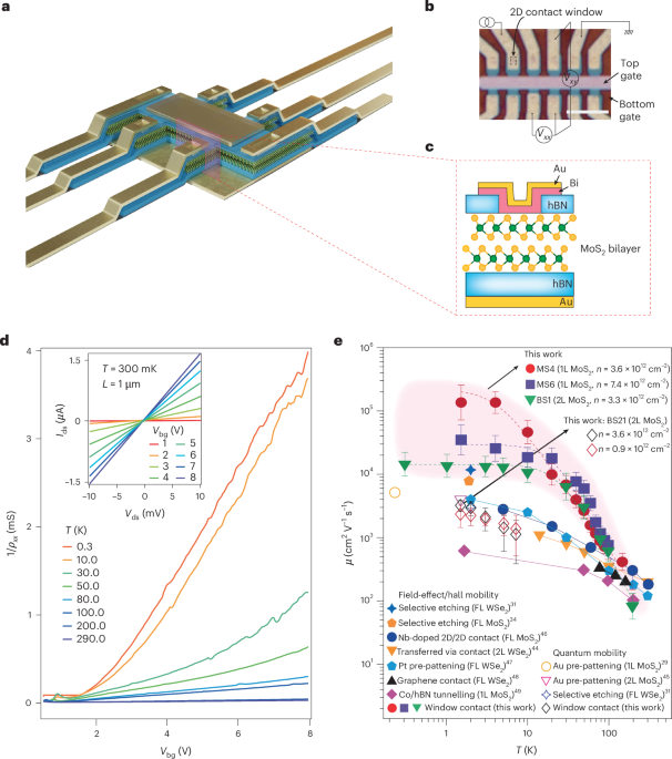
We solve the above challenges via windowed contact of bismuth to bilayer MoS2, with well-developed FQH plateaus seen in n-type MoS2 (Fig. 1), summarized below:
- We encapsulated bi-layered MoS2 between h-BN flakes, with the top h-BN pre-patterned with μm-sized holed windows. n-type semiconducting MoS2 with very low carrier density close to the band edge are thus achieved, by adopting the bismuth contact method with the delicate 2D-windowed evaporation process.
- Our DFT calculations and measurements consistently suggest that, when subjected to a finite vertical electric field Ez, the system behaves very much like a mono-layer MoS2 whose first four (lowest and first excited) LLs in the conduction band are layer-valley locked, and the spin-degeneracy is fully lifted by the Zeeman shift. This is because inter-layer tunneling only occurs in the valence band and is small compared to the band gap of MoS2, the layer index can thus be considered as a good quantum number for electrons in the conduction band in bilayer MoS2.
- We clarify that the negative slopes of LLs in the D-n map, in a typical asymmetrically Ohmic contacted bilayer MoS2 sample, is due to the fact that when the Fermi energy of the contacted top-layer comes in resonance with the opposite bottom layer’s conduction band edge, part of the electronic density is transferred to the top-layer without any contacts.
- We have demonstrated at 34 T and 300 mK, in multiple samples, FQH plateaus at ν = 4/5 and 2/5 in the extreme quantum limit in bilayer MoS2. This is the first transport experimental observation of well-defined FQH plateaus in high quality n-type TMDs. Notice that FQH plateaus in p-type TMDs have been recently reported. [9] Our theoretical modeling further explains the obtained hierarchy of FQH states in the current system.
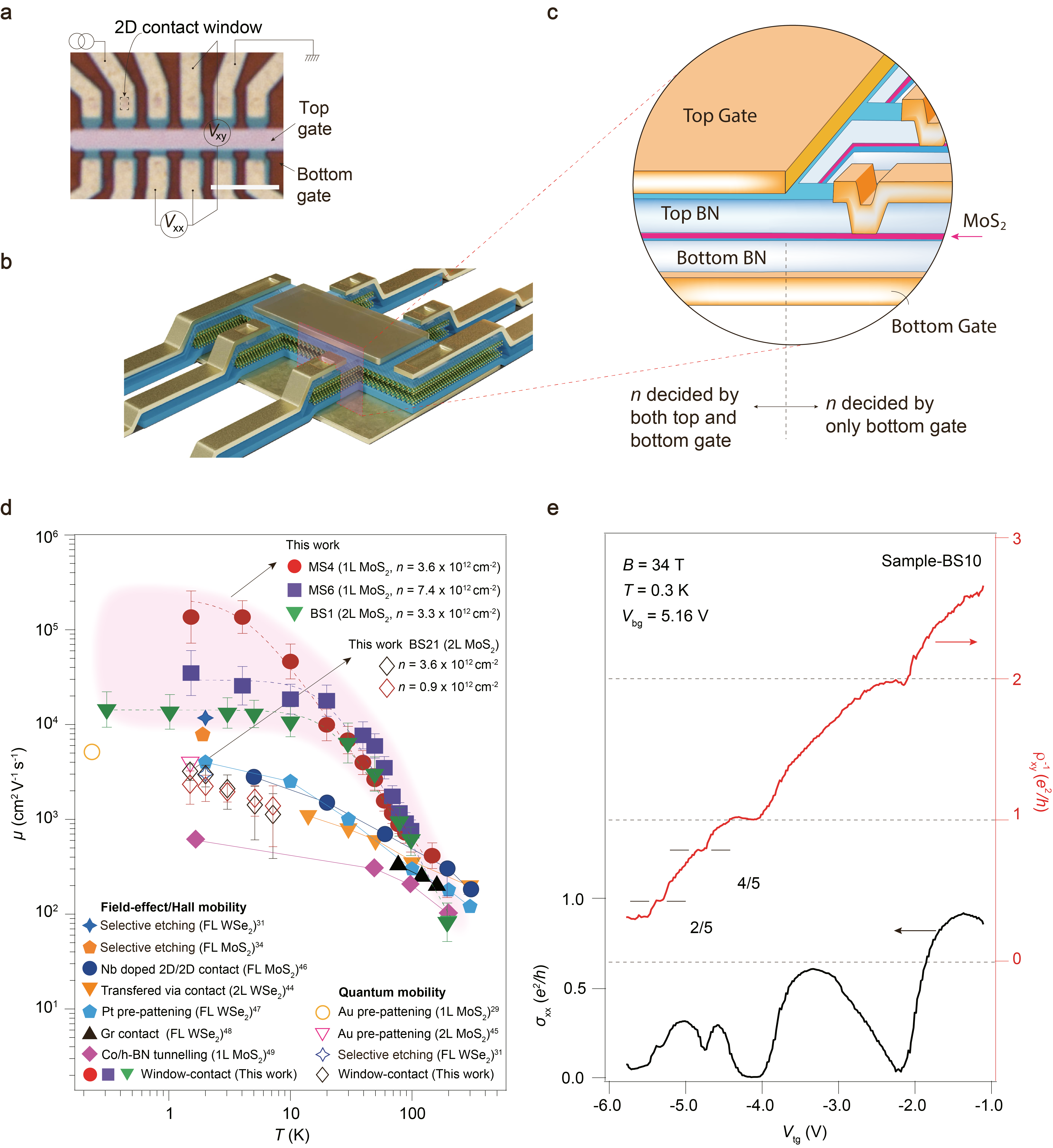
To summarize, our results show that n-type two-dimensional semiconductor material with a band gap (not in a topological flat-band system) can manifest fractional quantum Hall effect through electrical transport at high magnetic field and low temperature. These experimental results offer the possibilities for nano-electronic devices such as low-temperature amplifiers utilizing two-dimensional semiconductors, since they can behave like a low-temperature high-mobility electron transistor (HEMT). The latter are usually constructed by quantum wells.
For more details, please see the original version of the manuscript in Nature Electronics
https://www.nature.com/articles/s41928-024-01274-1
References:
[1] Klitzing, K. v. Dorda, G. and Pepper M. "New method for high-accuracy determination of the fine-structure constant based on quantized Hall resistance". Phys. Rev. Lett. 45, 494–497 (1980).
[2] Laughlin, R. B. "Anomalous quantum Hall effect: an incompressible quantum fluid with fractionally charged excitations". Phys. Rev. Lett. 50, 1395–1398 (1983).
[3] Du, X., Skachko, I., Duerr, F., Luican, A. & Andrei, E. Y. "Fractional quantum Hall effect and insulating phase of Dirac electrons in graphene". Nature 462, 192–195 (2009).
[4] Dean, C. R. et al. "Multicomponent fractional quantum Hall effect in graphene". Nat. Phys. 7, 693–696 (2011).
[5] Feldman, B. E., Krauss, B., Smet, J. H. & Yacoby, A. "Unconventional sequence of fractional quantum Hall states in suspended graphene". Science 337, 1196 (2012).
[6] Wu, Z. et al. "Even-odd layer-dependent magnetotransport of high-mobility Q-valley electrons in transition metal disulfides". Nat. Commun. 7, 12955 (2016).
[7] Masseroni, M. et al. "Electron transport in dual-gated three-layer MoS2". Phys. Rev. Res. 3, 023047 (2021).
[8] Han, Z. "Keep in contact". Science Bulletin 68, 787–790 (2023).
[9] Pack, J. et al. "Charge-transfer contacts for the measurement of correlated states in high-mobility WSe2". Nat. Nanotechnol. 19, 948–954 (2024).
Follow the Topic
-
Nature Electronics

This journal publishes both fundamental and applied research across all areas of electronics, from the study of novel phenomena and devices, to the design, construction and wider application of electronic circuits.
Please sign in or register for FREE
If you are a registered user on Research Communities by Springer Nature, please sign in