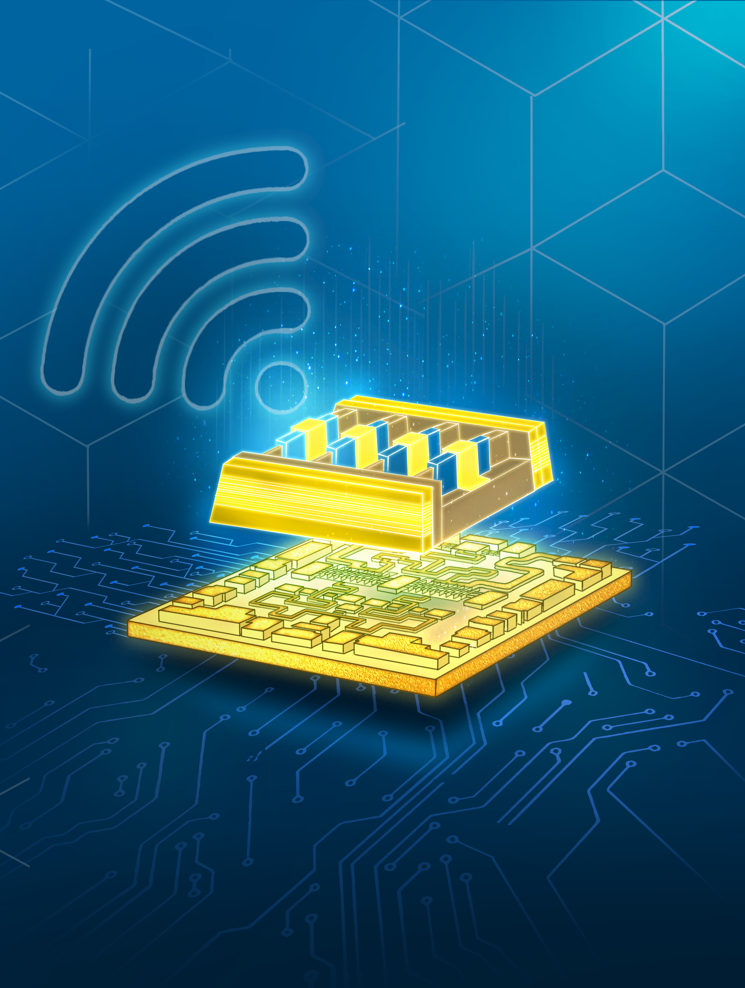
GaN Multichannel Transistors: The Next Revolution in RF Technology
Published in Electrical & Electronic Engineering and Materials
Future radiofrequency communication systems like 6G and phased-array transceivers need much greater data rates, higher resolution over larger distances and improved device reliability than current technology can provide. For example, state-of-the-art GaN single-channel transistors cannot meet these future requirements. These devices, called superlattice castellated field effect transistors (SLCFET), have demonstrated the highest W-band RF output power density reported in GaN technology. In particular, we have observed novel physics device effects, called the latch effect in SLCFETs, which has been thoroughly characterised and analysed using electrical and optical measurements, and 3D simulations. This work concludes that latch effects enable SLCFETs to demonstrate greatly enhanced RF power and linearity. The findings in this work are expected to bring SLCFETs into the limelight and encourage further research and development of GaN multichannel devices for future communication systems.
Conceptualization and Collaboration
The concept of SLCFETs was initially presented by Dr. Robert Howell from Northrop Grumman (NG) at the IEEE International Electron Devices Meeting in 2014. He demonstrated a field effect transistor (FET) based on a low loss and high isolation RF switch. The idea centred on a multichannel approach where up to 10 channels were stacked on top of each other. This structure helped reduce the on-resistance resulting in a very high switching figure-of-merit. In fact, SLCFET-based RF switches showed the highest figure-of-merit among any FET-based switch. The successful demonstration of the switch was a confidence boost in order to pursue the more fabrication-challenging SLCFET for amplifiers. Such an ambitious project needed collaborations, especially with researchers in academia. This initiated collaboration with Centre for Device Reliability (CDTR). The complimenting expertise paved the way for developing SLCFET amplifiers.
Device Fabrication and Testing
The devices were fabricated at Northrop Grumman, Linthicum, USA. The advanced fabrication facilities housed in a vibration-free class 100 cleanroom ensured the devices were fabricated with utmost precision and reproducibility. The device features had sub-100 nm dimensions. The real fabrication challenge was to achieve this uniformity over more than 1000 fins within the same device. This was achieved using advanced nanofabrication techniques like molecular-beam epitaxy, electron beam lithography, atomic layer deposition and inductively coupled plasma reactive etching. The entire process development of SLCFET amplifiers took more than 5 years to achieve the current maturity.
Testing of such complex structures at the CDTR in Bristol needed developing advanced testing strategies. We developed a noise analysis-based technique to screen out less reliable devices. This was highly efficient to rapidly and non-destructively identify devices which would fail early. Another novel testing technique is the use of electroluminescence (EL) from which the electron temperature of the device during RF operation can be estimated. This EL technique paved the way for understanding reliability challenges down to a single fin from over 1000 structures.
Overcoming Challenges
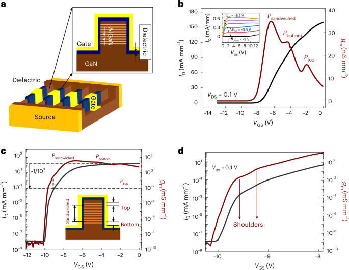
One of the key challenges was understanding the origin of the latch effect and its implication on device’s RF performance. Although the latch effect is observed in the sub-threshold regime of operation, its effect on the on-state performance was never understood. Again, there is no model available in a TCAD software to simulate this effect. The structures being sub-100nm in dimension and having a 3D nature of the active device area made this even more challenging to image.
To overcome these challenges, we came up with an innovative measurement technique where the electrical dynamics around the occurrence of the latch effect was experimentally captured. This was possible due to the occurrence of photoemission, i.e. electroluminescence, when a high electric field is applied. The emission from a single fin was very close to the noise margin that it could have been easily ignored. This prompted us to change our camera to one with greatly higher sensitivity and meticulously search for signals of photoemission emission at the latching point. Sometimes the faint emission was buried in the system noise, and it needed to be extracted using advanced signal processing techniques. This strategy was very vital to determine the exact location of the latch effect within a device and the physics involved during latching condition.
Significance and Applications
As per our measurements, the occurrence of the latch effect is proposed to result in the ability to increase the RF power of these devices along with more than doubling the device’s linearity. Large signal measurements performed by Northrup Grumman at similar operation conditions indeed confirmed that operating in latched conditions enabled SLCFETs to exhibit record output power among GaN technologies. In addition, the reliability testing performed showed that this operating condition is non-degrading in nature, paving the way for its practical application. This work demonstrates the benefits of collaboration between industry and academia.
Future Directions
It is now confirmed that SLCFETs under latching conditions is a safe operation regime which can be exploited by device designers to increase output power and simultaneously enable very high device linearity. There still needs attention to be given towards efficient heat extraction from these devices at such high power operation. In this future direction, our collaboration is already actively pursuing techniques like integration of high thermal conductivity materials with SLCFETs. Such a device successfully implemented and when operated under latching conditions is expected to further improve SLCFET’s performance for next-generation high power high frequency operations.
I lead the Center for Device Thermography and Reliability (CDTR) and am Director of the UKRI Innovation and Knowledge Centre (IKC) REWIRE at the University of Bristol. CDTR/REWIRE is a researcher center with 35+ international researchers working on semiconductor electronics (RF and power), specifically semiconductor growth and device fabrication, thermal management, electrical device design & testing and device reliability. A lot of thrust lies in new materials and new device systems such as GaN, GaN-on-diamond, and Ga2O3 for RF and power applications, ranging from communications, radar, automotive to carbon reducing technology net zero applications. The CDTR/REWIRE collaborates with numerous companies including Element-Six, Infineon, Northop Grumman, Qorvo, UMS, WIN Semiconductor and many others. We also run large UK Engineering and Physical Sciences Research Council (EPSRC) grants e.g. the Programme Grant GaN-DaME led the development of GaN-on-Diamond electronics, ULTRAlGaN develops vertical AlGaN based circuit brakers; the IKC REWIRE develops and commercializes next genration high voltage power electronics using wide and ultrawide bandgap semiconductors. I co-founded TherMap Solutions (https://www.linkedin.com/company/14799659) with two of my postdocs, to spin out key wafer characterization equipment developed as part of my research. I am presently its Chief Business Officer (CBO). I have been awarded a Royal Academy of Engineering Chair in Emerging Technologies, Fellow of IEEE, MRS, SPIE, IET and IoP in recognition of my contributions to the research community.
Follow the Topic
-
Nature Electronics
This journal publishes both fundamental and applied research across all areas of electronics, from the study of novel phenomena and devices, to the design, construction and wider application of electronic circuits.


Please sign in or register for FREE
If you are a registered user on Research Communities by Springer Nature, please sign in