A room-temperature gate-tunable bipolar valley Hall effect in molybdenum disulfide/tungsten diselenide heterostructures
Published in Materials

In monolayer transition metal dichalcogenides MX2 (M = Mo, W; X = S, Se), the valley degree of freedom offers additional freedom to develop optoelectronic devices. The electrons and holes in the K and K’ valleys—the local minima in the carrier energy band of opposite chirality in momentum space— have opposite out-of-plane Berry curvatures. This causes the intrinsic valley Hall effect (VHE), where the anomalous velocity (the in-plane velocity component perpendicular to the in-plane electric field) in one valley is opposite to the anomalous velocity in the other valley, resulting in a detectable Hall voltage Due to the opposite magnetic moments in the K and K’ valleys, these two valleys are optically addressable using circularly polarized light.
Most of the reported VHE experiments require either cryogenic temperature or plasmonic structures, which limits the potential for application in practical devices. it is also important to optimize the on/off ratio in a valleytronic transistor as well as conventional transistors.
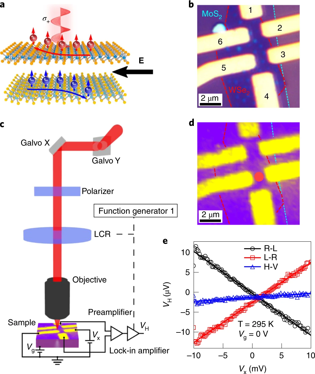
Based on the microscopic picture of the VHE in the 2D MoS2/WSe2, we fabricated MoS2/WSe2 heterostructure of AA-stacking alignment. Due to the MoS2/WSe2 type-II band alignment, the holes will stay in the WSe2 layer, whereas electrons undergo charge transfer to the MoS2 layer. This electron–hole layer separation suppresses intervalley scattering and reduces the exciton binding energy; both are beneficial for realizing VHE at a higher temperature. Figure 1 shows the VHE at room temperature with the device geometry and the experimental setup. Evidently, VH shows a linear dependence on Vx for circular polarization modulation (R-L and L-R). For linear polarization modulation (H-V), the value of VH is negligible.

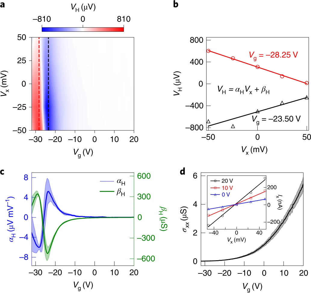
We measured the value of VH (right- minus left-circular polarization) by sweeping the Vg from −32 to 20 V at different Vx values ranging from −50 to 50 mV (Fig. 2a). The 220 μW, 726 nm excitation location is indicated as the red dot in Fig. 1d. Two linecuts (Fig. 2a) at Vg = −23.50 V and Vg = −28.25 V are shown in Fig. 2b. The data are fitted with the function VH = αHVx + βH. Here αH and βH are proportional to Hall conductivity and circular photocurrent (CPC), respectively. As shown in Fig. 2b, the sign of αH changes, indicating the change in VHE polarity. The plots of αH and βH as a function of Vg are shown in Fig. 2c. It shows that both polarity and magnitude of VHE are gate tunable, in contrast with VHE in the MoS2 monolayer, where only its magnitude is gate tunable. We also observe that the VHE and CPC are zero and optimum (that is, maximum or minimum) at the same gate voltage, indicating that they share similar photovoltaic mechanisms.

For more information, please visit our paper.
Follow the Topic
-
Nature Electronics
This journal publishes both fundamental and applied research across all areas of electronics, from the study of novel phenomena and devices, to the design, construction and wider application of electronic circuits.


Please sign in or register for FREE
If you are a registered user on Research Communities by Springer Nature, please sign in