Analogue in-memory computing coming of age
Published in Electrical & Electronic Engineering

Deep neural networks (DNNs) are at the forefront of the field of artificial intelligence (AI) due to their super-human capabilities in various cognitive tasks such as image recognition and text generation. However, the key challenge is that of running DNNs in a performant and energy efficient manner. While there have been significant advancements in specialized AI hardware, the shuffling of data between memory and processing units poses as the main hurdle towards that goal.
A radically different approach to addressing this challenge is by localizing the synaptic weights in terms of the conductance values of nanoscale resistance-based (memristive) storage devices and performing the synaptic computations in the memory arrays themselves. This architecture, called analogue in-memory computing (AIMC), like the human brain, obviates data movement between memory and processing units and therefore consumes significantly less energy. Moreover, the synaptic computations are performed in the analogue domain, exploiting circuit laws, for fast and energy efficient computations.
However, there are still key questions to be answered. Can this approach provide sufficient compute precision such that application accuracies are not impacted? Is it possible to seamlessly integrate analogue compute with digital compute, as a pathway towards full end-to-end realization of DNNs on-chip?
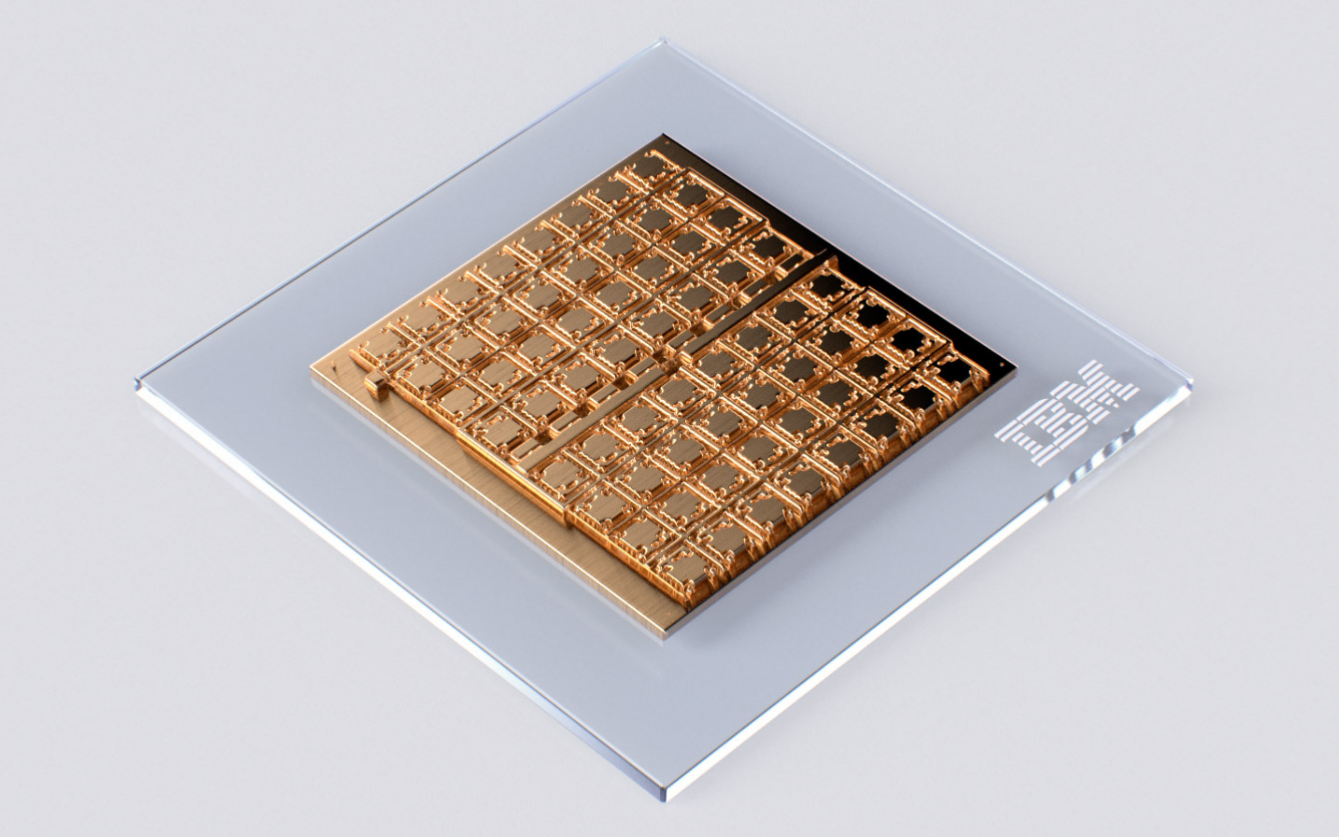
In our article, featured in Nature Electronics, we answer these questions by unveiling the first of its kind fully integrated mixed-signal in-memory compute chip based on back-end integrated phase-change memory (PCM) in a 14-nm complementary metal-oxide-semiconductor (CMOS) process. The chip comprises 64 AIMC cores (or tiles), each with a memory array of 256x256 unit cells. The unit cells are constructed with four PCM devices for a total of over 16M devices. In addition to the analogue memory array, each core contains a light digital processing unit performing activation functions, accumulations, and scaling operations. A global digital processing unit is placed in the middle of the chip for heavier digital computations associated with LSTM networks. Finally, an on-chip communication network enables core-to-core movement of partial results to enable accumulations.

The chip demonstrates massively parallel execution, with a maximal throughput of 63.1 tera-operations per second (TOPS), enabled by compact current-controlled oscillator Analog-to-Digital Converters (ADCs) placed on each unit-cell row. In the high-precision mode, using 4-phase read operation, the chip achieves 16.1 TOPS and the measured MVM throughput per area of the chip, 0.4 TOPS/mm2, is more than 15 times higher than comparable multi-core resistive memory AIMC chips.
The challenge in using PCM devices, however, is achieving sufficient computational precision. We characterized all 64 cores of the chip and demonstrated that they achieve an effective MVM precision between 3 and 4 bits. This is attributed to the proper on-chip ADC calibration circuits that remove unwanted nonlinear response. To assess whether the state-of-the-art MVM accuracy translates to inference accuracy, we implemented a variety of networks, covering all usable features of the chip.
First, we implemented a convolutional neural network for CIFAR-10 image classification. The network’s weights were programmed on 40 AIMC cores and the auxiliary network operations, namely batch normalization and ReLU activation, were implemented in the light digital processing units of the cores. Furthermore, accumulations of partial MVM results were also executed in the digital processing units, using the on-chip links to move the data between cores. The CIFAR-10 test accuracy achieved by the chip, 92.81%, is the highest amongst currently reported chips using similar technology.
In the next network, we aimed to answer the question “What is the achievable accuracy on a workload that utilizes all features of the chip?”. To answer that, we employed an LSTM network to generate captions of images in the Flickr8k dataset. The network utilizes all 64 cores, all digital processing units, and the on-chip communication network. In this case, the hardware accuracy, measured in BLEU scores, exactly matches the software floating-point baseline, despite of the full utilization of the chip.
As most fields transition towards AI-based technologies, the need for fast, low-power, and accurate inference hardware will be paramount. With the IBM HERMES project chip, we demonstrated that Analog-AI is a viable alternative to the conventional digital accelerator approaches. While further advances are required to mature the technology and move towards chips that can execute end-to-end inference workloads, this work demonstrates many of the building blocks needed to realize the full potential of Analog-AI.
Follow the Topic
-
Nature Electronics

This journal publishes both fundamental and applied research across all areas of electronics, from the study of novel phenomena and devices, to the design, construction and wider application of electronic circuits.


Please sign in or register for FREE
If you are a registered user on Research Communities by Springer Nature, please sign in