Atomically resolved imaging of radiation-sensitive metal-organic frameworks via electron ptychography
Transmission electron microscopy (TEM) is widely used for high-resolution imaging on nanomaterials. However, atomic-resolution imaging of electron beam-sensitive materials, e.g., zeolites, metal-organic frameworks (MOFs), covalent organic frameworks (COFs), and hybrid perovskites, presents a long-standing challenge,1–4 especially under scanning TEM (STEM) mode, where a convergent high-energy electron probe scans over the fragile samples, potentially causing irradiation damage to sample structures during imaging.
Electron ptychography, revitalized by advanced electron detector technologies that facilitate efficient acquisition of four-dimensional STEM (4D-STEM) datasets in these years, offers a promising solution to this challenge.5–7 It has several advantages over other imaging methods. For example, it is not restricted by the traditional numerical-aperture-limited resolution and has demonstrated superior resolution down to the deep-sub-angstrom level, also with greater tolerance to specimen thickness, establishing a new resolution record for real-space imaging. Moreover, it exhibits resolving power in the third dimension (i.e., depth resolution) at the nanometer level, which is difficult for conventional STEM to achieve. Additionally, electron ptychography does not require a perfectly aberration-free probe (especially the precise focusing) and utilizes almost all the signals available in the electron diffraction patterns. These features make it suitable for low-dose imaging on beam-sensitive materials.
However, considering that previously, most electron ptychography cases used electron dose of tens of, or even hundreds of thousand electrons per square angstrom (e-/Ų) and the damage threshold for MOFs or COFs is approximately 100 e-/Ų or even less, high-resolution imaging of these extremely beam-sensitive materials through electron ptychography has yet to be accomplished. The main challenge is that electron ptychography is a computational imaging method, which relies on the measured diffraction patterns and sophisticated algorithms to reconstruct the structural information of samples. At very low electron doses, great noise in the diffraction patterns may not lead the algorithms to a reasonable optimization way, resulting in reconstruction inferiority or even failures. In such cases, an optimal parameter setup that makes the best use of every electron for data collection should be explored and addressed. After our successful “moderately low-dose” (~3500 e-/Ų) imaging work on zeolites with iterated electron ptychography,8 we are focusing on further lowering the electron dose to apply it to atomic-resolution imaging on MOFs or COFs.
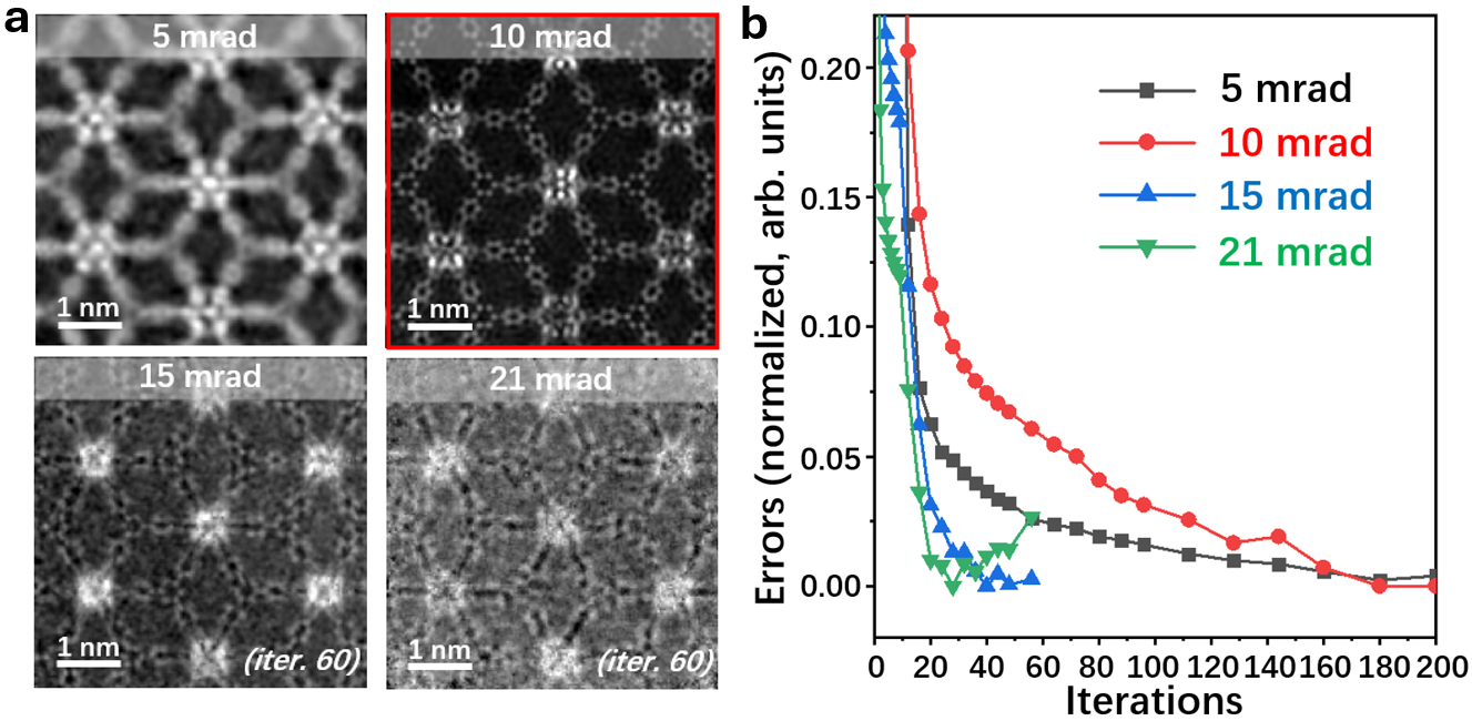
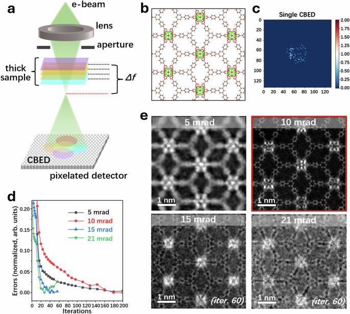
Fig.1 Analysis of the impact of 4D-STEM conditions on low-dose ptychography through simulations. a, reconstructed ptychography phase images using 4D-STEM datasets simulated at varying convergence semi-angles with a consistent electron dose of 100 e-/Å2. The 10 mrad case shows the best reconstruction, as marked by the red square. b, Iterative reconstruction error curves. Reconstruction of 15 mrad and 21 mrad failed after 60 iterations.
To address this, in this study, we explored the optimal parameters for MOF imaging with iterated 4D-STEM ptychography. Through simulations, we investigated the effects of the convergence semi-angle (α) of the probe on low-dose ptychographic reconstruction. Interestingly, different from most of the previous high-dose works on other materials that prefer a larger α for higher resolutions, a slightly smaller α, i.e., 10 mrad, instead, is suitable for low-dose imaging on MOFs (Fig. 1). We systematically analyzed the reasons behind. Firstly, the MOFs, characterized by large unit cells and open frameworks, do not require information transfer at very high spatial frequencies to effectively characterize their key structural features (10 mrad is enough at 300 kV). For a given limited total electron dose, a larger α value would allocate more signal to the high spatial frequency realm, at the expense of low frequencies, resulting in a weakened signal for reconstruction. Secondly, the convergence angle directly affects the probe size and depth of field. A small convergence semi-angle is helpful for the initial estimate of a defocused probe shape during the reconstruction, which is important for further iterated computation, especially for noisy datasets acquired at low doses. Moreover, for the experimental part, with a large convergence semi-angle, minor defocusing can result in a significantly enlarged probe size, risking exceeding the limits of the reconstruction box size and potentially leading to wrap-around artifacts or failed reconstructions. This issue in practical experiments can also be effectively avoided by employing a small convergence semi-angle.
![Fig.2 Experimental electron ptychography imaging of MOF MOSS-6. a, Ptychography phase image reconstructed from an experimental 4D-STEM dataset acquired at conditions of 10-mrad convergence semi-angle, 1.05 Å scan step, and an electron dose of 98 e-/Å2. b, The power spectrum of (a), demonstrating information transfer up to 1.96 Å. c, Enlarged image from the square-marked area in (a). d, Local region of the [001]-projected structure of NU-1000, a component of MOSS-6. Green/orange: Zr; red: O; gray: C; pink: H. Within each Zr cluster, the Zr pairs with strong and weak projected electrostatic potential intensity are labelled in orange and green color, respectively. The comparison between (c) and (d) indicates that the reconstructed ptychography phase image accurately reflects the MOF’s structural features, including the cluster orientation.](https://images.zapnito.com/cdn-cgi/image/metadata=copyright,fit=scale-down,format=auto,quality=95/https://images.zapnito.com/uploads/LQ05lmJTQn6p1FA4g5kR_fig.2.jpg)
Fig.2 Experimental electron ptychography imaging of MOF MOSS-6. a, Ptychography phase image reconstructed from an experimental 4D-STEM dataset acquired at conditions of 10-mrad convergence semi-angle, 1.05 Å scan step, and an electron dose of 98 e-/Å2. b, The power spectrum of (a), demonstrating information transfer up to 1.96 Å. c, Enlarged image from the square-marked area in (a). d, Local region of the [001]-projected structure of NU-1000, a component of MOSS-6. Green/orange: Zr; red: O; gray: C; pink: H. Within each Zr cluster, the Zr pairs with strong and weak projected electrostatic potential intensity are labelled in orange and green color, respectively. The comparison between (c) and (d) indicates that the reconstructed ptychography phase image accurately reflects the MOF’s structural features, including the cluster orientation.
With this guidance from simulations, we experimentally demonstrated the feasibility of effectively conducting 4D-STEM ptychography for highly beam-sensitive materials, exemplified by two MOFs, at low electron doses of ~100 e-/Å2 necessary to preserve their structural integrity, yielding directly interpretable images with a resolution of approximately 2 Å (Fig. 2). Thanks to the phase-contrast characteristic of ptychographic images, both metal clusters and organic linkers in MOF structures are observed simultaneously, with adjacent atomic columns of metal within the clusters clearly separated. The high resolution and contrast in the reconstructed images enable direct observation of various local structures of the MOFs, e.g., structural inhomogeneity and surface terminations. Overall, our study provides guidance and insights for imaging beam-sensitive materials using electron ptychography, by exploring its dose and resolution limits.
For further details, please refer to our paper “Atomically resolved imaging of radiation-sensitive metal-organic frameworks via electron ptychography” on Nature Communications (DOI: https://doi.org/10.1038/s41467-025-56215-z).
Reference
- Lv, J., Zhang, H., Zhang, D., Liu, L. & Han, Y. Low-Dose Electron Microscopy Imaging of Electron Beam-Sensitive Crystalline Materials. Acc. Mater. Res. 3, 552–564 (2022).
- Liu, L., Zhang, D., Zhu, Y. & Han, Y. Bulk and local structures of metal–organic frameworks unravelled by high-resolution electron microscopy. Commun. Chem. 3, 99 (2020).
- Zhou, Y., Dong, Z., Terasaki, O. & Ma, Y. Electron Microscopy of Nanoporous Crystals. Acc. Mater. Res. 3, 110–121 (2021).
- Ghosh, S., Kumar, P., Conrad, S., Tsapatsis, M. & Mkhoyan, K. A. Electron-Beam-Damage in Metal Organic Frameworks in the TEM. Microsc. Microanal. 25, 1704–1705 (2019).
- Jiang, Y. et al. Electron ptychography of 2D materials to deep sub-ångström resolution. Nature 559, 343–349 (2018).
- Chen, Z. et al. Electron ptychography achieves atomic-resolution limits set by lattice vibrations. Science 372, 826–831 (2021).
- Li, G., Zhang, H. & Han, Y. 4D-STEM Ptychography for Electron-Beam-Sensitive Materials. ACS Cent. Sci. 8, 1579–1588 (2022).
- Zhang, H. et al. Three-dimensional inhomogeneity of zeolite structure and composition revealed by electron ptychography. Science 380, 633–638 (2023).
Low-dose Transmission Electron Microscopy; 4D-STEM Ptychography
Follow the Topic
-
Nature Communications

An open access, multidisciplinary journal dedicated to publishing high-quality research in all areas of the biological, health, physical, chemical and Earth sciences.
Related Collections
With Collections, you can get published faster and increase your visibility.
Women's Health
Publishing Model: Hybrid
Deadline: Ongoing
Advances in neurodegenerative diseases
Publishing Model: Hybrid
Deadline: Mar 24, 2026


Please sign in or register for FREE
If you are a registered user on Research Communities by Springer Nature, please sign in