Blink and You Miss It: Cubic on the Outside, Chaotic Within
Published in Electrical & Electronic Engineering and Materials
Picture a semiconductor you can whisk up on a lab bench the way you brew a morning coffee, no furnaces roaring at a thousand degrees, no multimillion dollar clean rooms, and yet it can race neck and neck with the perfectly groomed Silicon and the III-V semiconductors. That, in a nutshell, is the miracle of the halide perovskites. How does a material born of such happy-go-lucky chemistry rival crystals raised with obsessive, monastic care? It’s a puzzle that has sent a whole field of scientists, including our team, into a deep and winding exploration.
The charm of being a little bit “dirty”
In most semiconductors, a stray misaligned atom is a mortal sin: every defect becomes a trap where energetic carriers, electrons and holes, fall in and die, bleeding away the current a solar cell needs. Halide perovskites, oddly, don’t seem to care. You can sprinkle them with defects and they still let charge zip across the film like impatient commuters catching the morning train to work. In the jargon, we call that defect tolerance: the ability to remain bright and conductive even when the lattice isn’t a model citizen.
Why the forgiving nature? Peer inside and the crystal looks less like a rigid mineral and more like a busy town square. The organic molecules stochastically reorient in their octahedral cages, ions hop under the lightest nudge, lone‑pair electron dynamics add to fuzziness along with the charge carriers that can dress the moving lattice to form polarons. The whole lattice hums with fluctuations.
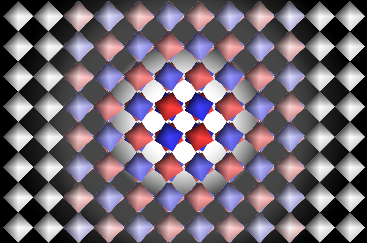
Standard textbooks treat vibrations, phonons, as neat, predictable notes on a violin string. Here, the instrument seems to be improvising jazz. Certain modes flare up, vanish, and pop back again, as if the material briefly locally shapeshifts into a tetragonal phase before settling once more into its cubic skin. In other words, rather than all phonon modes sharing comparable occupation at room temperature, Bose-Einstein statistics pour many more quanta into the anharmonic, soft, low-frequency modes; these become selectively amplified, with oversized oscillations that locally break the cubic symmetry, visible as low-symmetry nanodomains by freezing the lattice every trillionth of a second.

The journey into the unknown
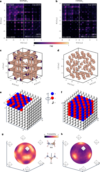
Our exploration of the hidden lattice dynamics in halide perovskites began with an attempt to steer a triple-axis neutron spectrometer through reciprocal space using phonon maps derived from DFT. Surprisingly, almost nothing appeared where the calculations predicted; most optical phonons had lifetimes too short to be registered by the instrument. Transitioning to Brillouin light scattering with Irina Kabakova solved this mystery. Suddenly, we could observe long-lived acoustic modes, which intriguingly shifted frequencies, either softening or hardening, depending on the type of A-site cation. These shifts suggested the existence of dynamic nanodomains, prompting us to draft a proposal to investigate these using diffuse X-ray scattering. Coincidentally, on the night we submitted our proposal, the first diffuse scattering map of CsPbBr₃ was published, confirming we were pursuing a promising direction.
Our subsequent synchrotron experiments soon revealed familiar patterns in methylammonium (MA)-based perovskites, yet the diffuse scattering pattern of formamidinium (FA)-based perovskites appeared strikingly different. After completing my PhD, I moved to the Stranks Lab, where discussions frequently revolved around octahedral tilting. At the time, PhD student Kieran Orr convinced me, guided by Glazer’s seminal work, that tilt perturbations naturally propagate in-plane within perovskites, resulting in two-dimensional sheets of tilted octahedra. Concurrently, Weadock et al. arrived at a similar conclusion based on their MA-based system's diffuse scattering data. Inspired, I built a model predicting diffuse scattering patterns generated by three-dimensional nanodomains with specific symmetry and shapes. The model worked beautifully for MA-based perovskites but couldn't quite capture the complexity we saw in FA-based systems.
Things took an interesting turn when James Neilson visited Cambridge and generously shared diffuse scattering data on FAPbBr₃, which contradicted ours. Intrigued, I applied our octahedral tilt model to Neilson’s data and discovered that FA-based systems have unique nanodomain symmetry and shapes, distinctly different from their MA-based counterparts. Motivated by these new insights, we remeasured FAPbBr₃, this time carefully controlling for potential beam damage. Our careful approach paid off. We successfully replicated Neilson’s dataset and learned a crucial lesson: although X-ray damage in halide perovskites seems subtle and doesn't significantly affect the average structure, it profoundly influences the local structure, creating distinctive diffuse scattering patterns.
Meanwhile, Aron Walsh’s group was independently developing machine learning-assisted molecular dynamics simulations of perovskite lattices. Once they extended their force fields to include organic A-site cations, Xia Liang and Johan Klarbring converted simulation MD trajectories into synthetic diffuse scattering patterns. Their simulations closely matched our experimental data, strongly validating our approach and deepening our understanding of these fascinating materials.
How dynamic nanodomains influence optoelectronic properties
Confident in the accuracy of molecular dynamics simulations, we started piecing together an atomistic picture of the lattice dynamics. This helped us understand why this unusual structural behaviour is so important for the optoelectronic performance of halide perovskites, proving exceptional in applications like solar cells, LEDs, and X-ray detectors.
We found that the dynamic appearance and disappearance of different symmetry phases dramatically shake up the electronic structure. Unlike typical semiconductors, where electrons have a steady, uniform probability of appearing throughout the crystal, in halide perovskites, electrons encounter "no-go" zones that appear and disappear every few picoseconds. This creates a constantly shifting electronic landscape, strongly modulating how charges move through the material.
We also discovered that the shape of these domains makes a big difference. In FA-based perovskites, these domains tend to be more spherical, reducing the overall disorder of the electronic landscape. Our experimental results backed this up, confirming the connection between domain shape, density and dynamic disorder of the electronic structure.
Outlook
The nanodomains we discovered are stacked in a regular pattern, much like ferroelastic twins observed in the low-temperature phases of perovskites such as MAPbBr₃. Thus, at room temperature, most halide perovskites consist of ferroelastic precursor nanodomains. Depending on their specific properties, these nanodomains can evolve into ferroelastic twins, leading to a ferroelastic phase transition, meaning their domain arrangements can be manipulated by applying mechanical stress.
Furthermore, our work suggests that dynamic ferroelastic twins present in the cubic phases of halide perovskites can also be altered under strain. Given our findings that optoelectronic properties are directly influenced by these nanodomains, applying external stress should similarly modulate their optoelectronic behaviour. This insight might explain why strain engineering is increasingly popular in the halide perovskite field. However, further experiments are necessary to conclusively demonstrate this link, potentially involving direct, real-time observation of electronic and structural fluctuations.
For more information, please read the full paper. If you have any questions feel free to contact me via email, Twitter or LinkedIn.
Follow the Topic
-
Nature Nanotechnology
An interdisciplinary journal that publishes papers of the highest quality and significance in all areas of nanoscience and nanotechnology.


Please sign in or register for FREE
If you are a registered user on Research Communities by Springer Nature, please sign in