Bridging the gap between printing and photolithography for molecular electronics and photonics with ‘molecular gates’
Published in Electrical & Electronic Engineering

Our paper Rapid and high-resolution patterning of microstructure and composition in organic semiconductors using ‘molecular gates’ was engendered by a pair of questions discussed with my supervisor, Mariano Campoy-Quiles, on the first day of my joining his group at the Institute of Materials Science of Barcelona (ICMAB-CSIC). “How can we pattern everything in organic semiconductors?” With photolithography or inkjet printing one patterns material composition, but micro-engineering of microstructure—e.g., molecular orientation, conformation, crystallinity—is generally unattainable. And yet the latter is immensely attractive for integrated devices: for instance, by patterning chain orientation one can unlock the inherently anisotropic properties of semiconducting polymers, and thus locally manipulate their electrical and thermal conductivities, as well as enabling polarised absorption and emission of light. Moreover, when selecting one of the existing patterning techniques one is inevitably faced with a choice: either rapid patterning of coarse features or slow, laborious high-resolution patterning.
And secondly: “What is your recipe for being creative?” After concluding that my approach starts with inventing an attractive brand name, the term ‘molecular gate’ appeared on the table. This project was then enabled by the synergy of the authors’ complementary expertise (Fig. 1): Mariano offered, among many creative insights, a wide-ranging experience with spectroscopic characterisation, while I contributed a toolbox of material science tricks learned at the infamous Polymer Technology group of Prof. Paul Smith, ETH Zürich.

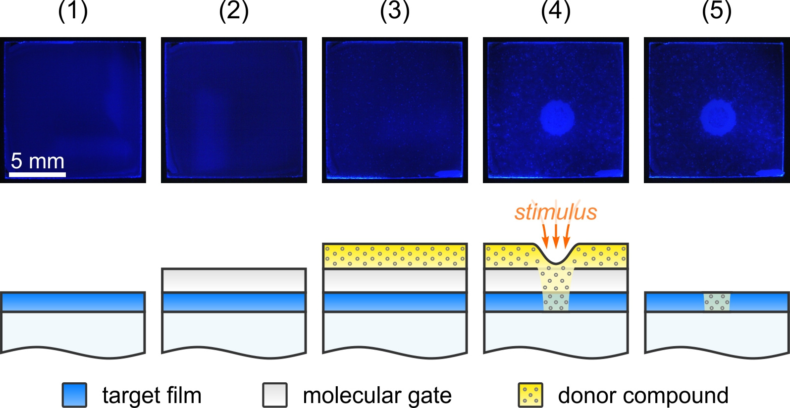
The concept of molecular-gate-based patterning is as versatile as it is simple (Fig. 2). Do you remember transferring an image with carbon paper? Now replace the canvas by a target molecular semiconductor, the carbon paper by a small-molecular donor layer (there are many more interesting things to transfer beyond graphite), and the thin layer of air that prevents the carbon paper automatically colouring your canvas by a thin ‘spin-on’ molecular gate. The molecular gate, besides protection, also temporally holds together the other two layers ensuring perfect alignment. Then, replace your pencil with a laser to, literally, write with light. As the final step, peel off the donor layer and molecular gate by ‘spin-off’ to reveal the microscopic piece of art.

Fig. 2 Sequential processing steps of molecular-gate-based patterning and exemplary fluorescence images for a light-emitting polymer film.
Key to realisation of patterning, therefore, is the selection of appropriate donor compounds to perform the desired type of patterning. For instance, crystallisable ‘solvents’ may be used to pattern molecular orientation by epitaxial solidification; other solid ‘solvents’ can be employed to manipulate chain conformation and crystallinity. Compounds such as light-emitting dies or dopants can be used to locally tune the optical or electrical properties of the target layer, respectively. Here one is limited only by creativity, with entire chemical catalogues at their disposal.
As the stimulus, one has the broad choice of using heat, solvent vapour jets or focused laser beams. In this first demonstration we report straightforward patterning of both composition and microstructure in several benchmark semiconducting polymers – with spatial resolution <5 μm and speeds up to 3 mm s–1 (Fig. 3). Further improvements are possible following additional process optimisation.

Fig. 3 Examples of laser-patterned features in semiconducting polymers.
“The fact that the method is based on molecular diffusion opens the possibility to modify the composition locally one molecule at a time—thus with extreme compositional accuracy—and that is why we say that our method introduces the concept of ‘molecule-on-demand’ into the low-cost, solution-based processing schemes” says Mariano. “Another unique trait of this technology is that it allows to pattern more than one functionality in a single step. One example is the production of pixels exhibiting three different emission colours obtained by controlled simultaneous diffusion of several small molecules into the target film.”
Ongoing research is proceeding jointly between ICMAB-CSIC and Karlsruhe Institute of Technology. A patent application has been filed on the method, and industrial partners are sought for joint co-development of this technology. Finally, we invite researchers from the field, as well as other disciplines, to contact us with challenging projects that may be advanced using the demonstrated molecular-gate-based approach.
In conclusion, if someone now asks me how we could pattern something in organic semiconductors, I would simply say: “Let's try with molecular gates.”
More details can be found here:
Nanostructured Materials for Optoelectronics and Energy Harvesting group; ICMAB-CSIC
Follow the Topic
-
Nature Communications
An open access, multidisciplinary journal dedicated to publishing high-quality research in all areas of the biological, health, physical, chemical and Earth sciences.
Related Collections
With Collections, you can get published faster and increase your visibility.
Women's Health
Publishing Model: Hybrid
Deadline: Ongoing
Biosensing
Publishing Model: Hybrid
Deadline: Jun 30, 2026


Please sign in or register for FREE
If you are a registered user on Research Communities by Springer Nature, please sign in