Crystallization control of drop-cast quasi-2D/3D perovskite layers for efficient solar cells
Published in Electrical & Electronic Engineering

Research into perovskite-based photoabsorbers for solar cells has exploded in the past decade. No other class of photoabsorber material has demonstrated such a rapid increase in efficiency, and efforts to further increase their device performance and extend their operating lifetime continue unabated. Since the first application of methylammonium lead halide in a dye sensitised solar cell, the metal halide perovskite family has dramatically increased in number, with new derivatives of hybrid organic inorganic perovskites and fully inorganic perovskites reported weekly.
As the physical properties of these perovskites can differ significantly, a researcher must weigh up the strengths and weaknesses of each material when determining what is most suitable for their application. Can it be deposited as a uniform thin film? Can it be processed in air? Is it stable under a wide range of conditions? One group of materials that satisfies each of these requirements is 2D perovskites.
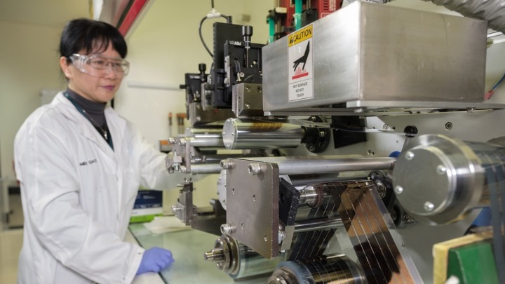
The Printed Photovoltaics Team in CSIRO Manufacturing is developing methods for the large-scale fabrication of organic and perovskite solar cells using solution-based deposition methods. The objective of this work is to significantly decrease the capital and energy requirements in producing solar cells in order to challenge the market dominance of c-Si solar cells. In 2019, this led us to investigate the deposition of 2D perovskites, which, although they demonstrate a lower efficiency than their 3D analogues, exhibit excellent environmental stability across a broad range of conditions. Furthermore, they could be deposited in air and still give impressive device efficiencies of up to 14.3%. However, if we are to increase their performance we need to improve the quality of the thin films by using additives in the precursor solution and optimising the deposition process to yield larger crystal grains.

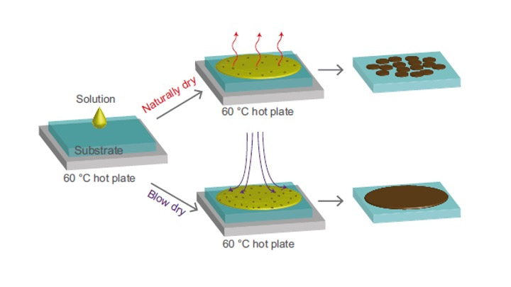
In this study, we test a range of drying conditions in conjunction with the use of a MACl additive, which suppresses the formation of lower order 2D-perovskite layers, to determine what parameters are required for uniform thin films. As any gaps in the perovskite film will cause shunting, which can cause significant decreases in device efficiency, this is an essential step in ensuring maximum photovoltaic performance. This is demonstrated by tests using uncontrolled drying under ambient conditions that yielded discontinuous films that give lower device efficiency, proving that proper consideration of the drying environment is required. As part of this study, we also expanded our understanding of the grain structure of the perovskite thin films using GIWAXS measurements performed at the Australian Synchrotron, which showed that incorporating the phenylethylammonium cation gives randomly oriented films, while use of iso-butylammonium gives the vertically oriented films that are required for enhanced performance.

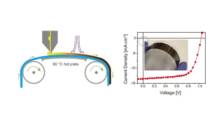
Overall, this study shows that combining the judicious selection of perovskite components with optimised deposition conditions can yield high efficiency and robust perovskite devices. This is a significant step towards realising the large-scale production of these devices using industry-relevant roll-to-roll printing processes.

Follow the Topic
-
Communications Materials

A selective open access journal from Nature Portfolio publishing high-quality research, reviews and commentary in all areas of materials science.
Related Collections
With Collections, you can get published faster and increase your visibility.
Advanced characterizations of high-entropy materials
Publishing Model: Open Access
Deadline: Jun 30, 2026
Engineering interface and low-dimensional superconductivity
Publishing Model: Open Access
Deadline: Apr 23, 2026


Please sign in or register for FREE
If you are a registered user on Research Communities by Springer Nature, please sign in