Hypotaxy: Downward Growth of Wafer-scale Single Crystal Transition Metal Dichalcogenide Films via Coalescence of Aligned Nuclei through graphene nanopores
Published in Materials
With the rapid advancement and increasing complexity of semiconductor fabrication technology, there is a compelling need for high quality semiconductor materials with superior electrical, thermal, and mechanical properties. However, the limitations of silicon-based semiconductors have become apparent, signaling a critical need for alternative materials that can sustain superior performance even at the atomic scale. Among the candidates, two-dimensional (2D) semiconductors, such as transition metal dichalcogenides (TMDs), stand out as promising successors due to their ability to maintain crystallinity at the nanoscale, satisfying the rigorous requirements of contemporary semiconductor industry. Despite their remarkable attributes, including excellent electrical, optical, and thermal performance even at ultra-thin dimensions, the commercialization of 2D semiconductors remains hindered by the challenges of achieving large-area, high-quality growth. While significant progress has been made in synthesizing TMDs to address scalability issues beyond exfoliation-based methods, these advancements are not yet sufficient for widespread industrial use. This moment marks a crucial turning point for the semiconductor industry, as the feasibility of 2D semiconductors' integration into practical applications will determine their role in shaping the next era of electronics.
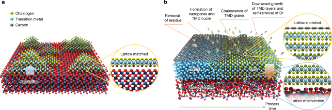
Chemical vapor deposition (CVD) is widely regarded as one of the most promising methods for producing 2D materials, including graphene and TMDs. Efforts to enhance the quality of CVD-grown TMDs have focused on achieving precise thickness control, enlarging grain size, and minimizing defects such as grain boundaries and vacancies. Among these approaches, the epitaxial growth of TMDs on highly crystalline substrates, such as sapphire, has gained significant attention [1-3]. This method allows TMD grains to grow in alignment with the crystal structure of the substrate, resulting in uniform, oriented growth. While epitaxy represents a major step forward in controlling crystal growth at the atomic scale, it is limited by the narrow selection of suitable substrates and the need for a transfer process to integrate the materials onto target platforms. Addressing these challenges is crucial for advancing monolithic 3D integration in semiconductor technology, emphasizing the importance of developing innovative and scalable synthesis methods.
We investigated the potential of utilizing a flexible, stable, and easily removable 2D material, rather than a conventional substrate, as the key factor determining the crystal orientation of growing materials. One of our key research focuses on functionalizing 2D materials to not only exhibit new properties but also enhance their interactions with other materials, enabling aligned growth driven by forces stronger than van der Waals interactions. Specifically, we developed a method to create nanopores in 2D materials, such as graphene and hexagonal boron nitride (paper in preparation, [4-7]), discovering that these intentional defects can activate unique forces in interactions with other materials. By leveraging this phenomenon, we predicted that such structural modification could serve as effective guides for the growth of other materials. Furthermore, through years of extensive work, our efforts included growing various 2D materials via CVD [8-10], leveraging interlayer interactions to strengthen the coupling between 2D materials and other substances, and achieving recrystallization or crystal orientation alignment between materials [11-13]. Beyond the traditional concept of epitaxy, we aimed to establish an integrated approach that allows 2D materials to be more freely studied and utilized in a wide range of applications. Our previous research culminated in the development of hypotaxy, with the prefix "hypo" meaning "downward" and the suffix "taxy" meaning "arrangement".
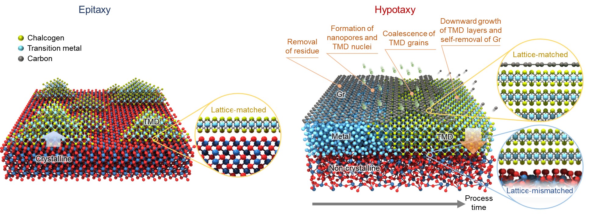
Figure 1. Growth mechanisms of epitaxy and hypotaxy. Schematics of growth mechanisms for conventional epitaxy (left) and proposed hypotaxy (right).
Interestingly, we found a key insight into the origins of hypotaxy during an experiment designed for an entirely different purpose. The initial aim was to employ the sulfurization of molybdenum (Mo) films - one of the simplest methods to synthesize large-area MoS2 - while using graphene as a barrier to block sulfurization in areas covered by graphene. This approach was intended to fabricate patterned MoS₂ structures during synthesis, but it unexpectedly provided critical clues to understanding the hypotaxial growth mechanism. We observed that the Mo was not sulfurized and remained beneath the multilayer graphene as we intended, while in regions covered by a single graphene layer, the graphene disappeared, and a single crystal of MoS2 was formed. The metal chalcogenization process is widely known as a simple method for synthesizing large-area TMDs, but has the problem with typically yielding poor-quality materials, so our unexpected result was surprising. We began to develop this process, termed hypotaxy, by closely observing the growth dynamics under progressively extended sulfurization durations.
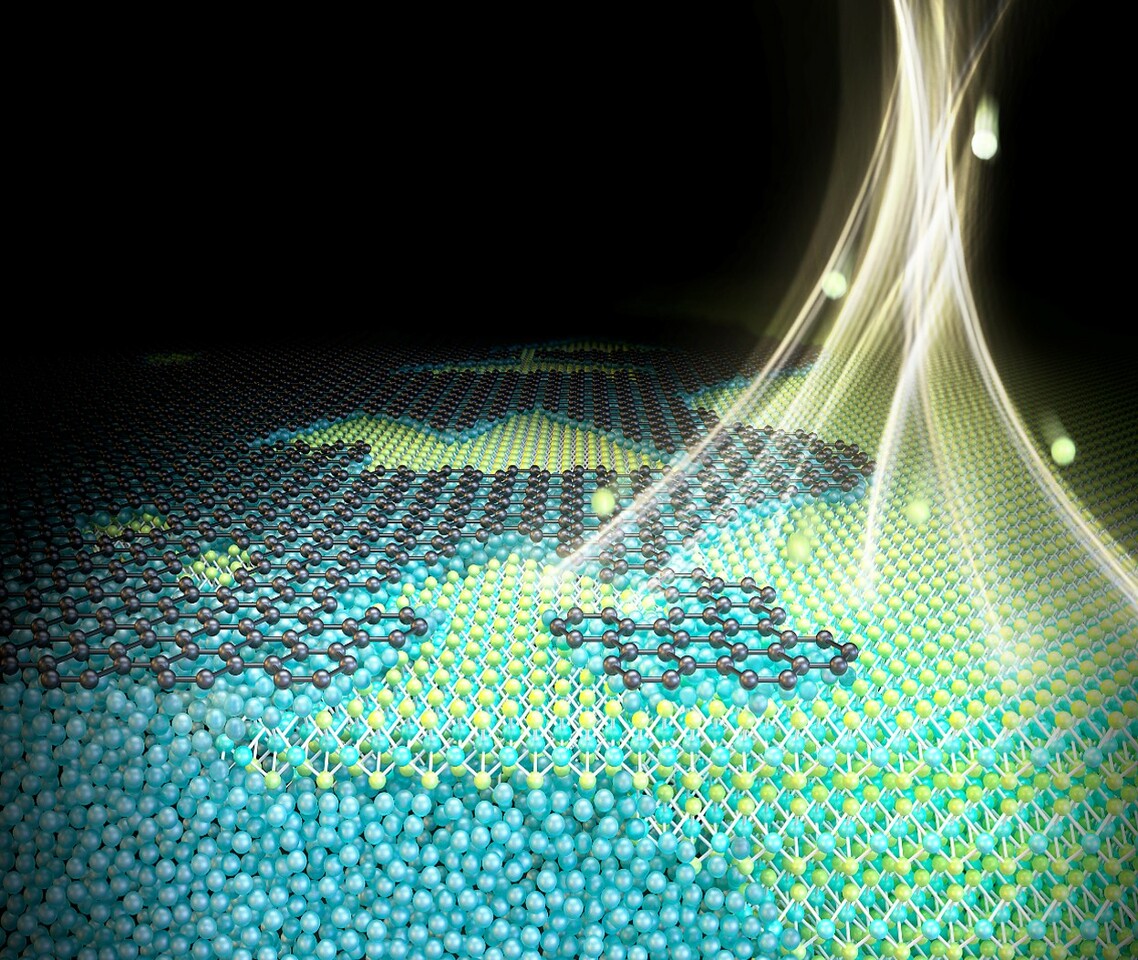
We found that the wafer-scale single crystal TMDs, such as MoS2, MoSe2, WS2, and WSe2, can be grown by sulfurization (or selenization) of pre-deposited transition metal films (Mo and W) through single crystal monolayer graphene that was transferred onto the metal films before sulfurization process. During the process, precursors, such as S and Se, are supplied through nanopores of < 5 nm in graphene that are generated in the beginning stage, and the MoS2 nuclei form with crystalline alignment with graphene. For hypotaxial growth, the formation of nanopores in the 2D templates, such as graphene and hBN, is critical. We revealed that nanopores of < 5nm in graphene have strong interaction with the growing TMD nuclei, leading to alignment of these nuclei. As the nanopores expand, the unidirectionally aligned MoS2 nuclei coalesce into larger grains without formation of grain boundaries. The MoS2 layers grow from the top region of the Mo film, remaining the Mo film at the bottom. Finally, the top graphene layer is removed naturally during the process, resulting in the formation of single crystal TMDs. The residue induced during graphene transfer is removed as well, leaving behind ultraclean surface of TMDs. Our hypotaxial growth technique enables us to fabricate 4-inch single crystal TMDs through overlying 2D templates even on amorphous or lattice-mismatched substrates, while preserving interlayer crystalline alignment with the 2D templates.
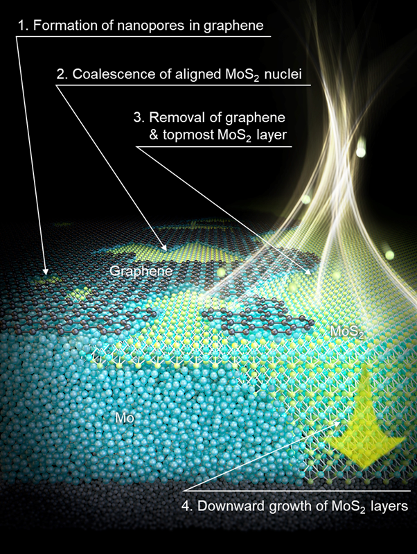
Figure 2. The step-by-step schematic of the hypotaxial growth of TMD through a two-dimensional template. By chalcogenization of a pre-deposited metal film under graphene, aligned TMD nuclei form, coalescing into a single-crystal film as graphene is removed.
This method achieves precise MoS₂ thickness control from monolayer to hundreds of layers on diverse substrates, producing 4-inch single-crystal MoS2 with high thermal conductivity (~120 Wm-1K-1) and mobility (~87 cm2V-1s-1). These properties are close to theoretical limits or higher than those of exfoliated samples. Additionally, nanopores created in graphene via oxygen plasma treatment allow MoS2 growth at a lower temperature of 400 °C, compatible with back-end-of-line (BEOL) processes. This hypotaxy approach also extends to other TMDs, such as MoSe2, WS2, and WSe2, offering a novel solution to substrate limitations in conventional epitaxy and enabling wafer-scale TMDs for monolithic 3D integration.
For more details, please see the original version of the manuscript in Nature.
(https://www.nature.com/articles/s41586-024-08492-9)
[1] Li, T. et al. Epitaxial growth of wafer-scale molybdenum disulfide semiconductor single crystals on sapphire. Nat. Nanotechnol. 16, 1201-1207 (2021)
[2] Liu, L. et al. Uniform nucleation and epitaxy of bilayer molybdenum disulfide on sapphire. Nature 605, 69-75 (2022).
[3] Kim, K. S. et al. Non-epitaxial single-crystal 2D material growth by geometric confinement. Nature 614, 88-94 (2023).
[4] Son, J. et al. Atomically precise graphene etch stops for three dimensional integrated systems from two dimensional material heterostructures. Nat. Commun. 9, 3988 (2018).
[5] Ryu, H. et al. Fluorinated Graphene Contacts and Passivation Layer for MoS2 Field Effect Transistors. Adv. Electron. Mater. 8, 2101370 (2022).
[6] Shin, Y. et al. Graphene Via Contact Architecture for Vertical Integration of vdW Heterostructure Devices. Small 18, 2200882 (2022).
[7] Shin, Y. et al. Facilitated fluorination and etching of 2D materials. Appl. Surf. Sci. 645, 158857 (2024).
[8] Jung, Y. et al. Nucleation and Growth of Monolayer MoS2 at Multi-steps of MoO2 Crystals by Sulfurization. ACS Nano 17, 7865-7871 (2023)
[9] Kwon, J. et al. 200-mm-wafer-scale integration of polycrystalline molybdenum disulfide transistors. Nat. Electron. 7, 356–364 (2024).
[10] Jung, Y. et al. WOx-driven growth of 2H- and 3R-WS2 multilayers by physical vapor deposition. Appl. Surf. Sci. 682, 161676 (2024).
[11] Kim, H. et al. In-plane anisotropy of graphene by strong interlayer interactions with van der Waals epitaxially grown MoO3. Sci. Adv. 9, eadg6696 (2023).
[12] Lee, Y. et al. Quasi-van der Waals Epitaxial Recrystallization of a Gold Thin Film into Crystallographically Aligned Single Crystals. ACS Appl. Mater. Interfaces 15, 6092-6097 (2023).
[13] Baek, J.-H. et al. Thermally induced atomic reconstruction into fully commensurate structures of transition metal dichalcogenide layers. Nat. Mater. 22, 1463–1469 (2023).
2D materials
Follow the Topic
-
Nature

A weekly international journal publishing the finest peer-reviewed research in all fields of science and technology on the basis of its originality, importance, interdisciplinary interest, timeliness, accessibility, elegance and surprising conclusions.


Please sign in or register for FREE
If you are a registered user on Research Communities by Springer Nature, please sign in