Single-nm MTJs Achieve High-Speed, High-Retention Performance
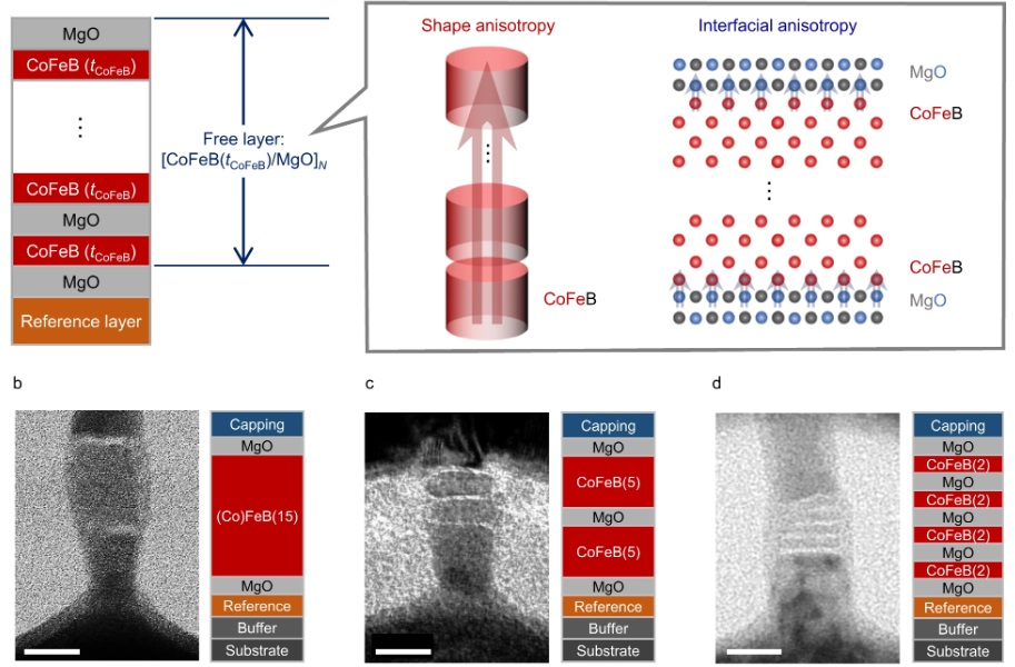
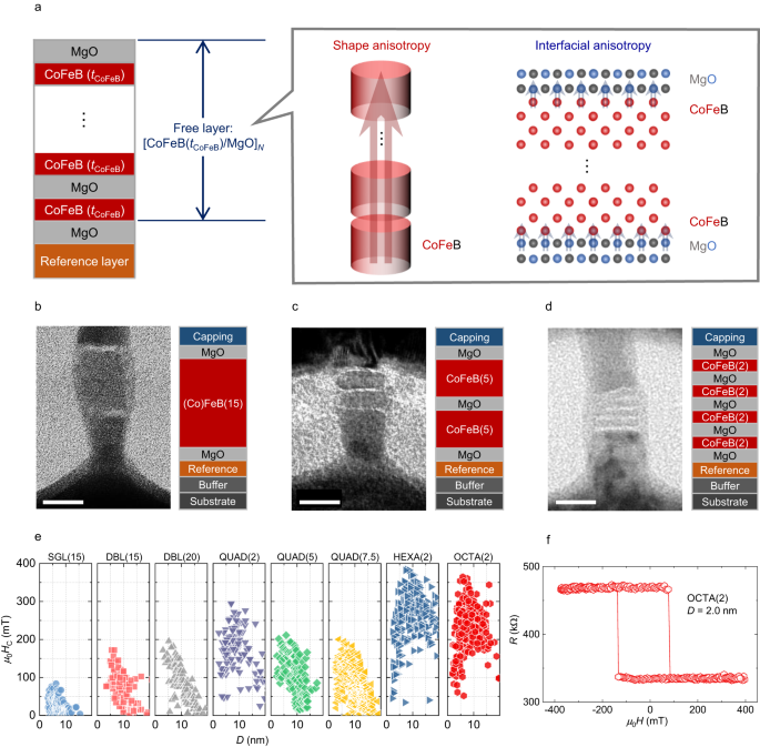
Spin-transfer torque magnetoresistive random access memory (STT-MRAM) is emerging as a promising technology, with potential to replace conventional memory types like SRAM, DRAM, and Flash. A key component of STT-MRAM is the magnetic tunnel junction (MTJ), which requires performance tuning for different applications. The challenge lies in achieving both fast speed for SRAM-like applications and long data retention for Flash-like applications, while also addressing scalability issues. Now a new study by Junta Igarashi and colleagues has made significant strides in this area by developing single-nanometer MTJs using a multilayered ferromagnetic structure that allows independent control of shape and interfacial anisotropies.
Igarashi et al.'s research presents a novel design of CoFeB/MgO multilayers as the free layer in MTJs. By varying the thickness of CoFeB layers (t) and the repetition (N) of CoFeB/MgO layers, they achieved precise control over the retention and switching speed performance. The study demonstrated sub-ten-nanosecond STT switching and over ten-year retention capabilities in single-nanometer MTJs with different stack designs. This was accomplished through meticulous fabrication processes, which included sputtering system deposition, electron beam lithography, reactive ion etching, and Ar ion milling.
The results showed that by increasing N or t, the thermal stability factor at room temperature was enhanced due to positive effects from both interfacial and shape anisotropies. For high-temperature applications such as automotive or embedded memory systems, the researchers tailored MTJs to emphasize shape anisotropy for better temperature insensitivity. Conversely, for speed-critical applications requiring fast STT switching within nanoseconds, they focused on enhancing interfacial anisotropy.
In summary, Igarashi et al. concluded that their approach to designing MTJs with multilayered ferromagnetic structures allows for tailored performance suitable for both high data retention and high-speed applications in the single-nanometer regime. The main advance made by this research is providing a design guideline for fabricating ultra-small MTJs that can be used across a wide range of technologies.
The ability to independently control interfacial and shape anisotropies at such small scales could lead to more efficient and versatile memory devices. This advancement may pave the way for further miniaturization of electronic components while maintaining or even improving their performance—a critical step forward as demands for faster processing speeds and higher storage capacities continue to grow in various technological fields.
This text on an editorially selected paper was initially drafted using artificial intelligence, and then fact-checked and improved by an editor to meet Springer Nature publication standards.
Follow the Topic
-
npj Spintronics
This is a fully open access journal publishing research articles that advance the understanding and application of spin electronics or spintronics.
Related Collections
With Collections, you can get published faster and increase your visibility.
Magnonics: from conventional to hybrid and quantum systems
Publishing Model: Open Access
Deadline: Jun 18, 2026
Techniques and Methods in Spintronics
Publishing Model: Open Access
Deadline: Aug 20, 2026





Please sign in or register for FREE
If you are a registered user on Research Communities by Springer Nature, please sign in