Spray-coated Perovskite Hemispherical Photodetector Featuring Narrow-band and Wide-angle Imaging
Published in Materials
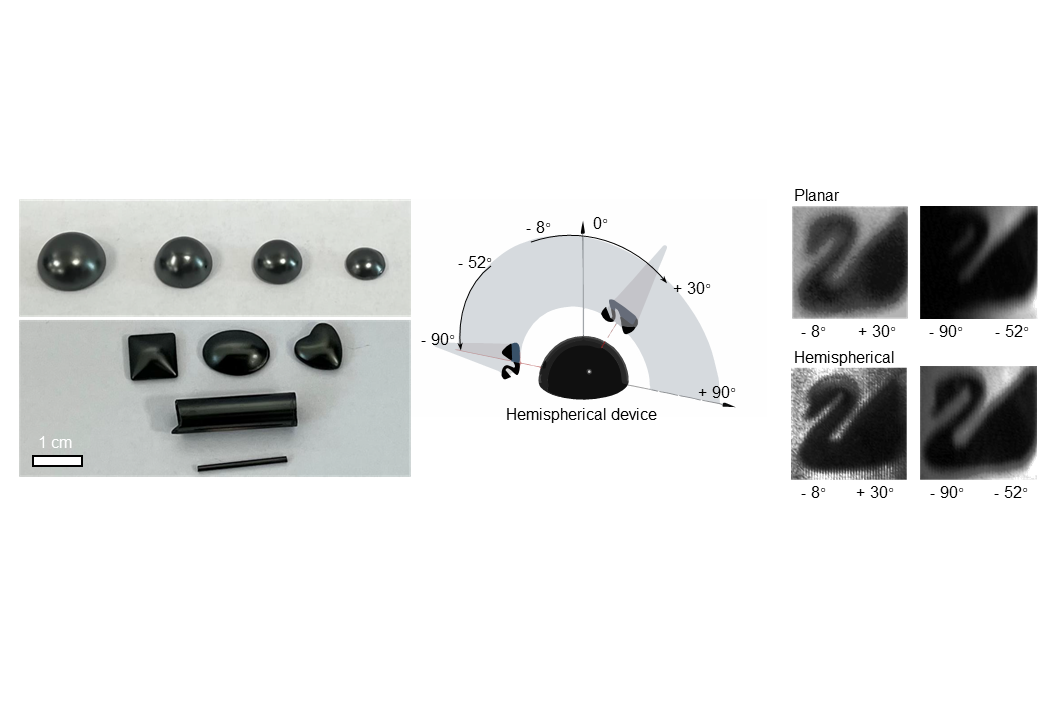
The research on developing curved and wavelength-recognition photodetectors is an essential section at present. Because of the geometrical shape, photodetectors with hemispherical surfaces have many advantages, such as wide-angle detection, stereo detection. Figure 1 shows the effective incident flux intensity at the hemispherical and planar surfaces. However, the fabrication of curved photodetector through traditional insoluble semiconductors is a challenge with the high cost and low efficiency. Nowadays, researchers are developing new semiconductor materials which can be dissolved in water or organic solvent and fabricated devices by an easy solution process. Among these materials, hybrid perovskites are the ideal materials with unique optoelectronic properties of anisotropic quantum confinement, tunable bandgap, and defect tolerance nature.
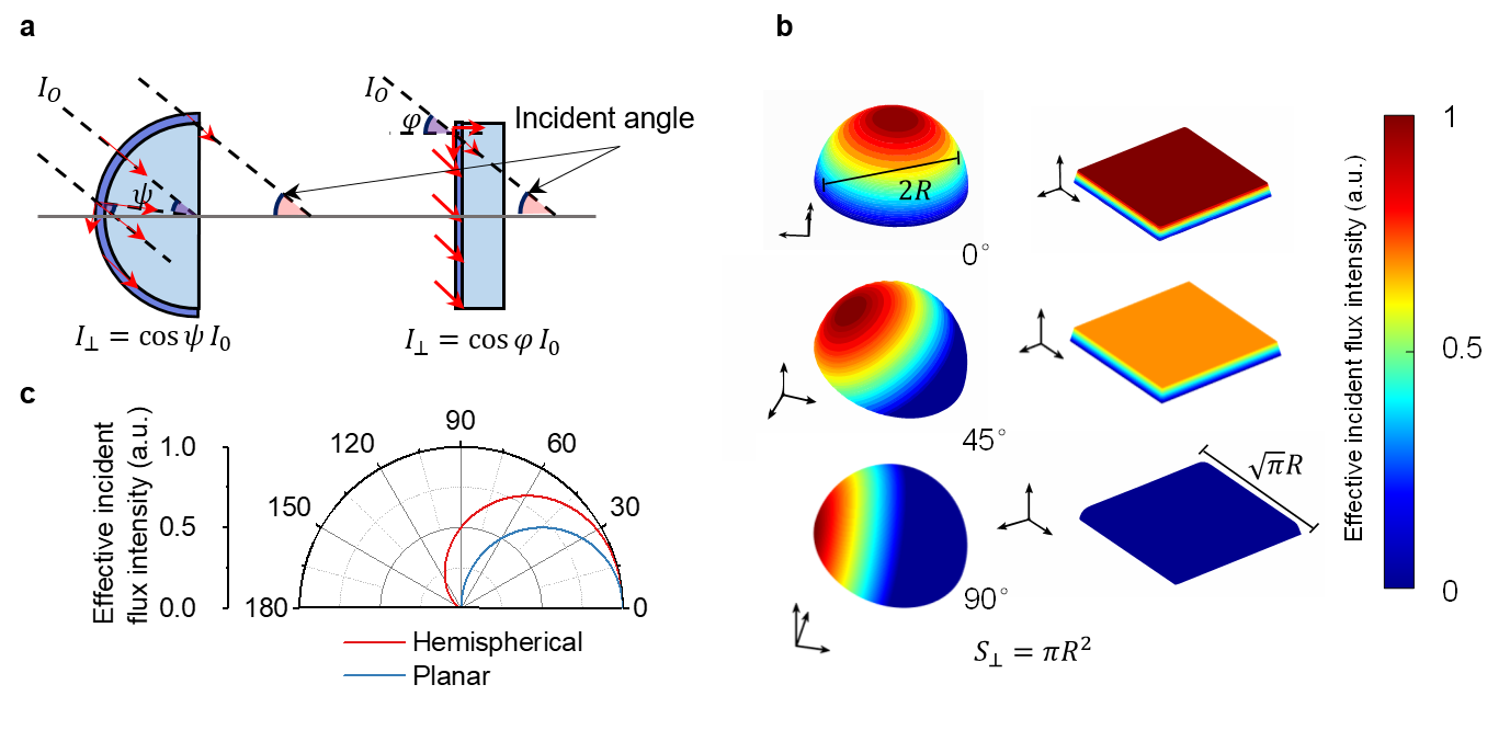
Figure 1 | The effective incident flux intensity of hemispherical and planar surface. a, Schematic diagram of the vertical component of incident light on hemispherical and planar surface. The incident light (red arrow) is decomposed into components parallel and perpendicular to the surface. ψ and φ are angles to evaluate the angle of incident light. b, The simulated spatial distribution of effective incident flux incident of planar and hemispherical surface (I⊥) under incident light from 0°, 45°, and 90°.c, The integrated flux under incident light from incident light from different angle.
To obtain the advanced photodetectors, researchers (X. Feng, H. He, W. Qu, J. Song, W. Pan, M. Tan) led by Prof. H. Wei and Prof. B. Yang at Jilin Unversity chose the quasi 2D perovskites as photoactive materials and spray-coating methods to fabricate a wide-angle and narrow-band photodetector without any optical filter. The solubility of solvents was tuned to ensure that the deposition of materials was layer-by-layer. The distribution of the flow field of the spray-coating and mechanical polishing was applied to obtain uniform films. The thickness of perovskite films is tunable by controlling the amount of the perovskite precursor. The velocity of spray-coating cycles is fast at 1.28 × 10⁻⁴ cm3 s-1 , with good repeatability.
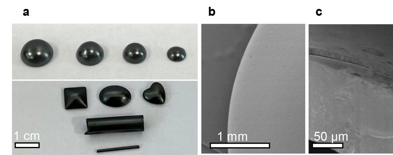
Figure 2 | The thick perovskite film fabricated by spray-coating. a, The optical photographs of spray-coated perovskite (PEA2FA3Pb4I13) films deposited onto different substrates of different sizes and shapes. b, The SEM image of the surface of the perovskite film on hemispherical substrate. c, The cross-section SEM image of the perovskite film on curved substrate.
The recombination in the films is adjustable by controlling the ratio of 2D components and the thickness of films without changing the bandgap of photoactive materials. It was proved that the 2D species exist in the grain boundary of the 3D perovskite. Thus, the carriers generated by short wavelengths can be recombined by organic layers, and defects lead to the narrow-band response. The full width at half maximums (FWHMs) of photodetectors is ~ 20 nm which is narrower than commercial band-pass filters. The Br-/I- ratio was controlled with a response from 550 nm (Green) to 820 nm (Near-infrared).
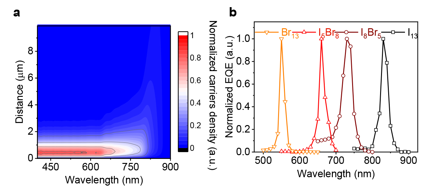
Figure 3 | Narrow-band response of photodetectors. a, The charges density of PEA2FA3Pb4I13 film at different wavelength and positions simulated by diffusion length and absorbance spectrum. b, The narrow-band response (EQE) of perovskites photodetectors with different halogen ratio (PEA2FA3Pb4I13, PEA2FA3Pb4I8Br5, PEA2FA3Pb4I5Br8, and PEA2FA3Pb4Br13).
The object with the shape of a swan was chosen to image by a single-pixel hemispherical detector and a homemade motorized positioning system under different monochromatic light to simulate the color imaging. Wide-angle imaging is also obtained by changing the direction of the photodetector. It was confirmed that the detection range of the hemispherical photodetector is near 180°. The researchers also fabricated a preliminary micro-array device to realize imaging under single light illumination like natural daylight or moonlight, which is a crucial step for further application. Photodetector arrays with 9×9 pixels (1.21 mm2) were fabricated with simple imaging. The researchers also restructured the image on a hemispherical surface rather than a planar surface, which is closer to curved imaging.
This article reported a perovskite narrow-band hemispherical photodetector through a fast spray-coating process, which performs lens-free imaging capability at a wide angle of nearly 180°. The researchers believed that this work is a good example of developing soluble semiconductor materials through the spray-coating process and solvent engineering, and there should be many exciting applications of photodetectors with curved structures.
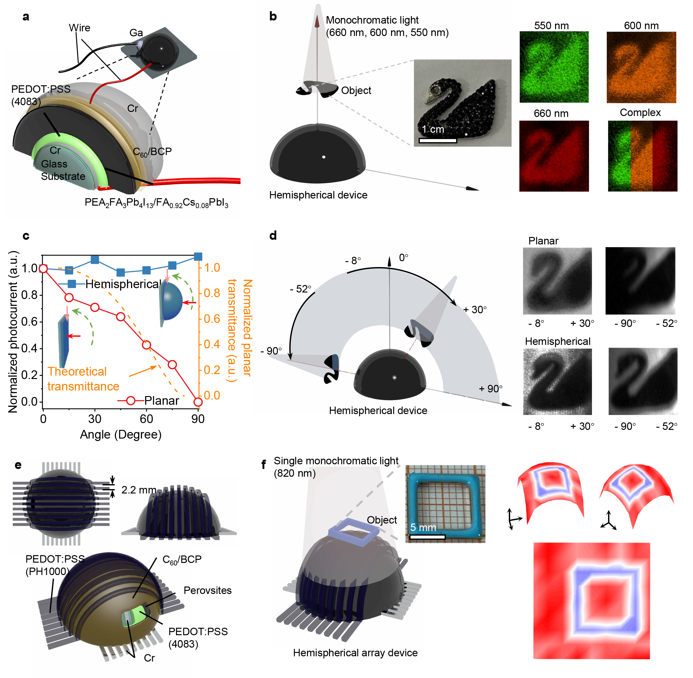
Figure 4 | Narrow-band and Wide-angle imaging of a hemispherical photodetector. a, The device structure of the hemispherical photodetector. b, Left: The schematic of the imaging system and the optical photo of a swan as object. Right: The images captured by hemispherical photodetectors with different I/Br ratios. The colors of images are matched to the color function. c, The photocurrent of hemispherical photodetector under irradiation from different angles (The size of the light source is smaller than the area of photodetectors.). The orange line is the relationship between the theoretical normalized transmittance and the incident angle of a planar perovskite film surface. d, Left: The schematic of the imaging system for wide angle detection. Right: The images captured by planar and hemispherical photodetectors based on different angles of incident light. e, The schematic of the structure of the micro-array (9×9) device f, Left:The schematic of the imaging system and the optical photo of a square plastic object. Right : The micro-array imaging result.
For more details, please see “, Spray-coated Perovskite Hemispherical Photodetector Featuring Narrow-band and Wide-angle Imaging, Xiaopeng Feng, Yuhong He, Wei Qu, Jinmei Song, Wanting Pan, Mingrui Tan, Bai Yang and Haotong Wei*”, Nature Communications, 2022, 13, 6106. https://www.nature.com/articles/s41467-022-33934-1
Follow the Topic
-
Nature Communications
An open access, multidisciplinary journal dedicated to publishing high-quality research in all areas of the biological, health, physical, chemical and Earth sciences.
Related Collections
With Collections, you can get published faster and increase your visibility.
Women's Health
Publishing Model: Hybrid
Deadline: Ongoing
Biosensing
Publishing Model: Hybrid
Deadline: Jun 30, 2026




Please sign in or register for FREE
If you are a registered user on Research Communities by Springer Nature, please sign in