Two-dimensional materials based transistors using hexagonal boron nitride dielectrics and metal gate electrodes with a high cohesive energy
Published in Materials
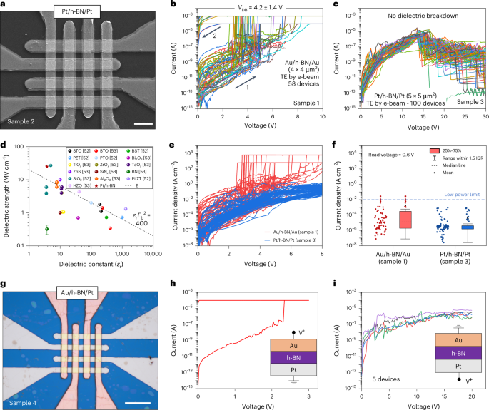
We have found that Pt/hBN gate stacks show 500-times-lower leakage current than Au/hBN gate stacks, and that they exhibit a high dielectric strength of at least 25 MV/cm. The data on the leakage current for small devices can be found in Figure 1 below. The rest of data can be found in the paper, available at the link provided.
The similitude with previous technology advancements is fascinating! In the early 2000, many companies experimented with high-k dielectrics as a potential replacement of ultra-thin SiO2 gate dielectric. However, most attempts failed due to the poor compatibility of high-k dielectrics with the adjacent materials. On that time, many experts stated that high-k materials will never make it. In 2004, Intel found that the introduction of high-k gate dielectrics required tuning the composition of the gate electrode, and they shifted from polysilicon to metal. Intel started to commercialize this technology in 2008, and all scaled transistors are now based on the high-k/metal gate technology.
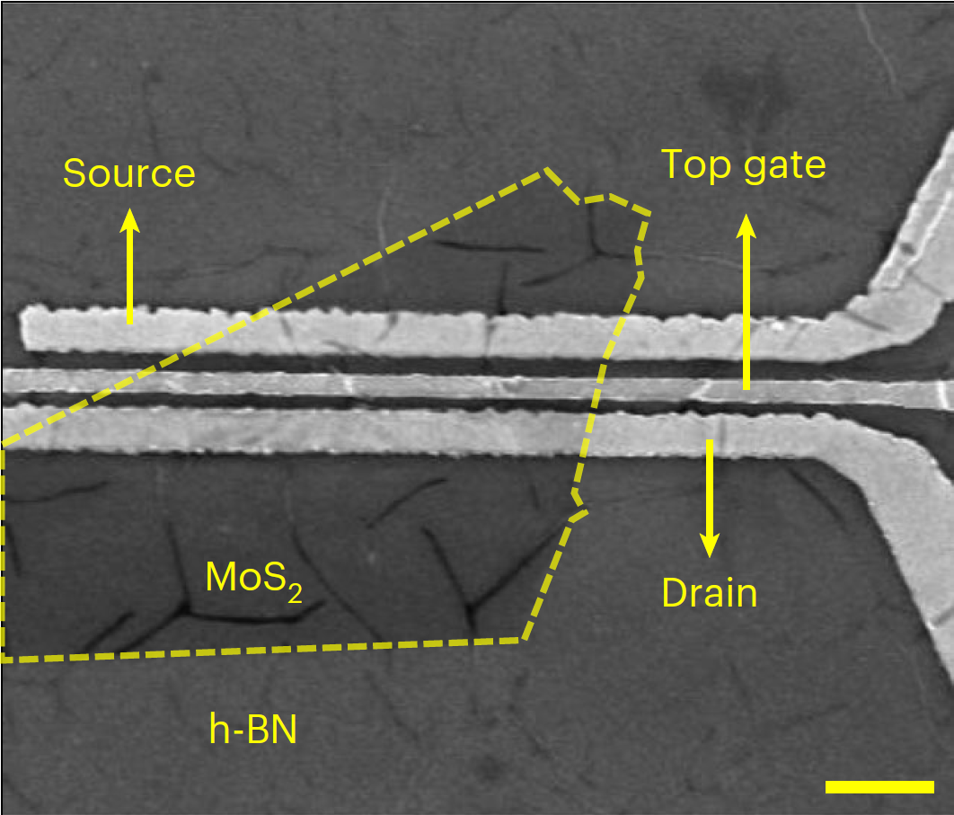
Now, when many people thought that hBN is a bad gate dielectric, we find that selecting the proper metal electrode enables its use as gate dielectric in field-effect transistors with MoS2 channels. And this is very interesting because MoS2 and hBN are very good friends: they can form a clean van der Waals interface for improved reliability.
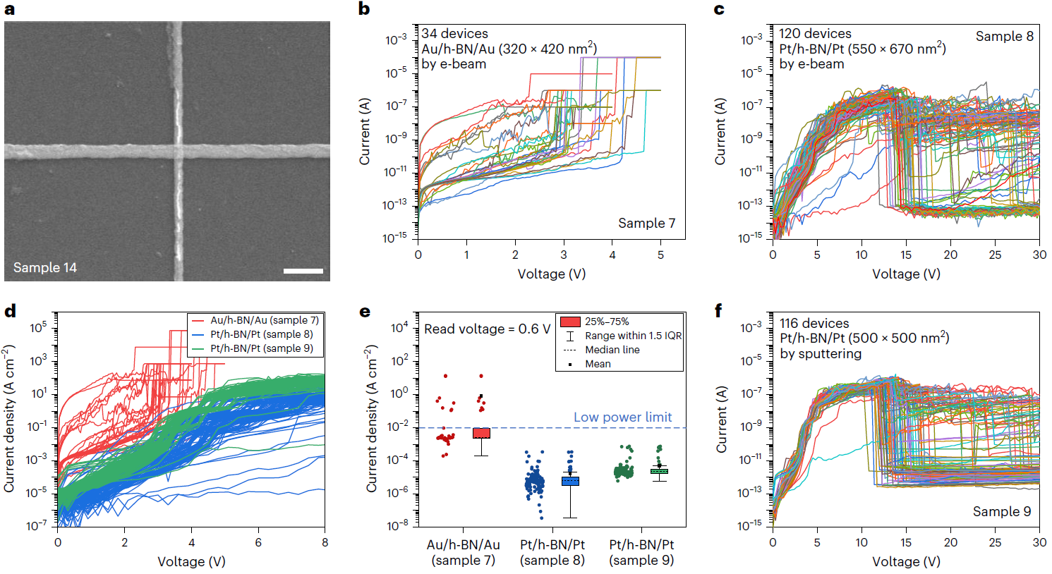
Figure 1 | Dielectric breakdown and leakage current in small Pt/h-BN/Pt and Au/h-BN/Au devices. (a) SEM image of the cross-point Pt/ h-BN/Pt device (device size 370 nm × 250 nm). Scale bar: 1 µm. (b) Current versus voltage characteristics measured in Au/multilayer h-BN/Au with lateral size of 320 nm × 420 nm, Au electrodes were deposited by electron beam evaporation. (c) Current versus voltage characteristics measured in Pt/multilayer h-BN/Pt with lateral size of 500 nm × 500 nm, Pt electrodes were deposited by electron beam evaporation. (d) Current density vs. voltage characteristics measured in Au/multilayer h-BN/Au and Pt/multilayer h-BN/Pt devices. (e) Box line distribution of current density of Au/multilayer h-BN/Au and Pt/multilayer h-BN/Pt devices. Each plot displays the median value (central line) and the 25th to 75th percentiles (box boundaries). The whiskers extend to a range of 1.5 times the interquartile range (IQR), beyond which outliers are marked as individual points. (f) I-V curve measured in Pt/h-BN/Pt with lateral size of 500 nm × 500 nm with Pt electrodes deposited by magnetron sputtering. Thickness of h-BN is ~8 nm.
Follow the Topic
-
Nature Electronics
This journal publishes both fundamental and applied research across all areas of electronics, from the study of novel phenomena and devices, to the design, construction and wider application of electronic circuits.


Please sign in or register for FREE
If you are a registered user on Research Communities by Springer Nature, please sign in