Controlling light emission from semiconductor nanoplatelets using surface chemistry

In our recently published paper, “Controlling Light Emission from Semiconductor Nanoplatelets Using Surface Chemistry”, my colleagues and I describe how the surface ligands on semiconductor nanoplatelets influence their optical properties, particularly the rate of light emission and the emission linewidth. This research represents a significant step forward in the field of nanotechnology, with potential applications in lighting, displays, photodetectors, quantum information, and more. In this blog post, I’d like to share the story behind our work.
Semiconductor nanoplatelets are tiny sheets, only a few atoms thick. About 3,000 nanoplatelets laid end-to-end, or 50,000 stacked on top of each other, would be as wide as a human hair. Like any semiconductor, these nanoplatelets can absorb energy when an electron jumps across the band gap, leaving a hole behind. This energy is later released, either electrically (if the electron and hole are separated, driving a current) or optically (if the electron and hole recombine, emitting a photon). This process is the foundation of all optoelectronics.
To make a solar cell or a photodetector, you design a device in which the incoming energy is light and electrical energy is released. If the incoming energy is electrical and light is emitted, you have an LED, a laser, or a quantum emitter. Nanoplatelets are particularly useful for optoelectronics because the thickness of the nanoplatelet determines the band gap and therefore the energy of the absorbed or emitted light. This means that you can change the color of emitted or absorbed light just by making the nanoplatelets thinner or thicker. The size and shape of nanoplatelets also encourage the electron and hole to form a bound state, called an exciton. Excitons absorb and emit light very quickly, resulting in brighter and more efficient optoelectronics.

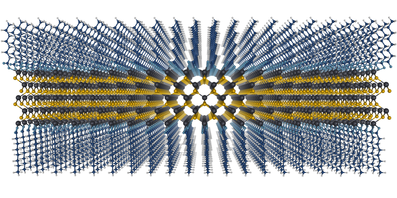
Atomistic visualization of a 4-monolayer CdSe nanoplatelet passivated by octanoate ligands. Cd is gray, Se is yellow, O is light blue, C is dark blue, and H is white.
Ideally, nanoplatelets would emit or absorb light at a single frequency, i.e., have a narrow emission or absorption linewidth. This is desirable for more vibrant colors in displays, for high-resolution photodetection, and for applications in quantum information, where precise control over the emission properties is critical. However, nanoplatelets show some variation in the energy of the emission. Previously, nobody knew what was causing this broadening. A team of scientists at the US Naval Research Laboratory—myself, Dr. Sasha Efros, and Dr. Steve Erwin—set out to understand this puzzle.
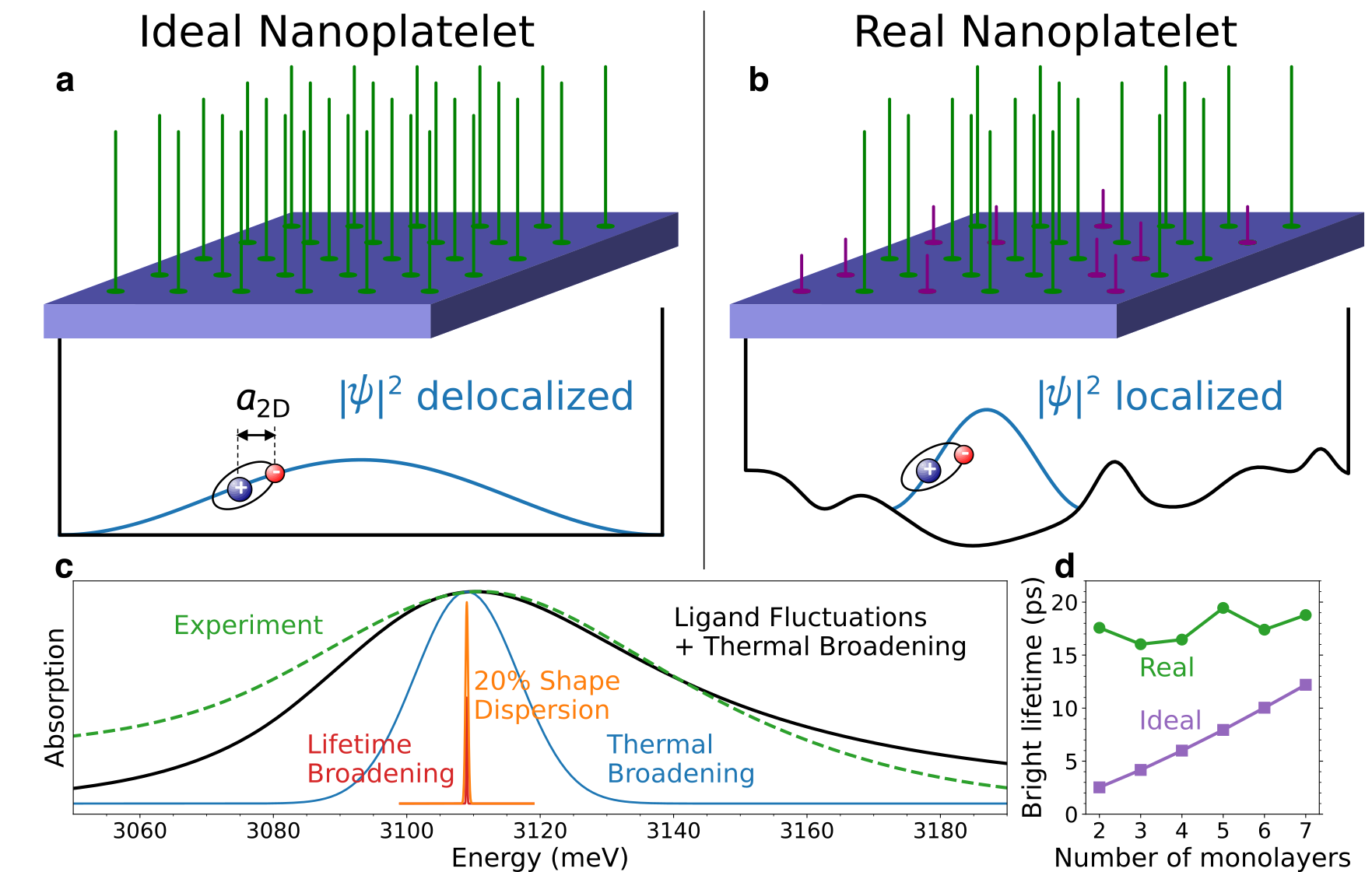
The ground-breaking insight came from the field of semiconductor quantum wells. A quantum well is a very thin layer of a semiconductor (call it type a) sandwiched inside a different type of semiconductor (type b), and in many ways behaves similarly to a nanoplatelet. Researchers found that if a few atoms of type b are mixed into the type a layer, this causes broadening of the emission lines. This happens because the disorder traps excitons in certain areas of the quantum well, rather than allowing them to move freely. This introduces variation in the energy of the emitted photons, i.e. broadens the emission lines, as well as slows the rate of emission.
Could a similar type of disorder be broadening the emission in nanoplatelets? Right away, we ruled out variations in thickness. Nanoplatelets are grown with very precise thickness control, down to an exact number of atomic layers (typically 2, 3, 4, 5, or 6). Furthermore, variations in thickness would cause much bigger linewidths than what is seen experimentally. We also ruled out variation in lateral size: the resulting linewidth would be far too small. What other type of non-uniformity could there be?
We came to consider surface chemistry. Most nanoplatelets are prepared in a liquid solution, with organic molecules (ligands) bound to the surface to protect them from the environment. Could non-uniformity in the ligand shell lead to broadening? It could! We estimated the size of this effect and found that the effect size was just right to explain experimental observations.
All that remained was to figure out what was the most likely type of non-uniformity in the ligands and to make some quantitative predictions. At first, we thought that some of the surface sites might be missing a ligand. However, after we discussed this idea with some experimentalists, we concluded that it was unrealistic: a bare site would be extremely reactive, so any initially bare sites would react (with a precursor, a solvent molecule, or an impurity in the solution) and end up passivated in some way. We concluded that the disorder must be caused by mixing different types of ligands. For example, standard nanoplatelet synthesis uses a mixture of short-chain and long-chain ligands when synthesizing nanoplatelets. There could also be unintentional ligands, caused by impurities in the solution or by unexpected reactions of surface sites with solvent atoms. For our research, we picked one specific example of ligand type fluctuations and computed the resulting linewidths in detail, both as a function of the mixing fraction between the two types, and as a function of the thickness of the nanoplatelet. We found that, in addition to broadening the emission, ligand disorder caused the excitons to emit more slowly, decreasing brightness and efficiency.

In conclusion, our study sheds light on the critical role of surface chemistry in controlling the optical properties of semiconductor nanoplatelets. More uniform ligand layers will sharpen the lines and speed the emission, unlocking the potential of these nanomaterials for new optoelectronic technologies. We are eager to continue exploring this growing field and look forward to the exciting new discoveries that lie ahead.
Follow the Topic
-
Nature Communications

An open access, multidisciplinary journal dedicated to publishing high-quality research in all areas of the biological, health, physical, chemical and Earth sciences.
Related Collections
With Collections, you can get published faster and increase your visibility.
Women's Health
Publishing Model: Hybrid
Deadline: Ongoing
Biosensing
Publishing Model: Hybrid
Deadline: Jun 30, 2026


Please sign in or register for FREE
If you are a registered user on Research Communities by Springer Nature, please sign in