Flatchat | Dirac plasmon-assisted asymmetric hot carrier generation for room-temperature infrared detection
Published in Electrical & Electronic Engineering

1. Could you briefly outline the key findings of your paper?
Ans: Low carrier mobility CVD grown large area graphene is turned into a highly sensitive, dynamically tunable, long wave IR detector.
2. What is your role in this work?
Ans: Project leader, concept generation, data analysis and overall project management.
3. What was the genesis of this paper? How did you come to this particular problem?
Ans: Our first goal was to make graphene absorb IR light strongly. A bare graphene film/ flake absorbs mere <2% light across the spectrum and quite useless as an IR detector material. By exciting cavity-coupled Dirac plasmons, we could enhance absorption to > 50% in mono-layer CVD grown graphene.
The next challenge was to separate change carriers as a function of IR absorption - graphene being a zero bandgap material is not possible directly. We developed an asymmetric hot carrier generation scheme which allowed us to generate thermoelectric voltage and detection IR photons efficiently.
4. What is the most empowering implication of your results?
Ans: At present all highly sensitive IR detectors (InSb, HgCdTe etc) need cryogenic cooling which makes them very expensive and show limited operational suitability. On the other hand microbolometers type uncooled mid-IR detectors are slow and lack sensitivity for low concentration chemical detection and high quality infrared imaging.
• II-VI, III-V and microbolometers are 30 years old technologies
• Evolutionary/incremental improvements to the existing state of the art
• Can we look for new material systems for uncooled infrared detection?
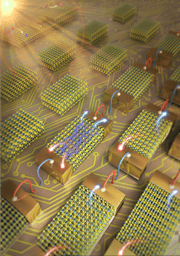
In this context, the proposed work is revolutionary since the proposed graphene based detection scheme promises uncooled, tunable and fast mid-IR detection in the technologically important 8-12 micron band.
5. How have 2D materials been uniquely instrumental to enabling these results?
Ans: The detection scheme offers ultrafast response time (τ ~ 10-9 sec) due to the high carrier mobility of graphene at room temperature. The proposed scheme offers dynamic tunability of the absorption as a function of applied gate voltage enabling path towards frequency selective IR detection and hyperspectral IR imaging. We demonstrate an asymmetric plasmon-induced hot-carrier Seebeck photodetection scheme at room temperature that exhibits a remarkable responsivity of 2900 VW-1, detectivity of 1.1x10⁹ Jones along with an fast response of ~ 100 ns in the technologically relevant 8 – 12 µm band. This is achieved by engineering the asymmetric electronic environment of the generated hot carriers on chemical vapor deposition grown large area nano-patterned monolayer graphene, which leads to a temperature gradient of 4.7 K across the device terminals for an incident power of 155 nW, thereby enhancing the photo-thermoelectric voltage by manifold compared to previous reports. The results presented outline a strategy for uncooled, tunable, multispectral infrared detection.
6. Can you describe the main challenges associated to the preparation of this manuscript? Any anecdotes you’d like to share with us?
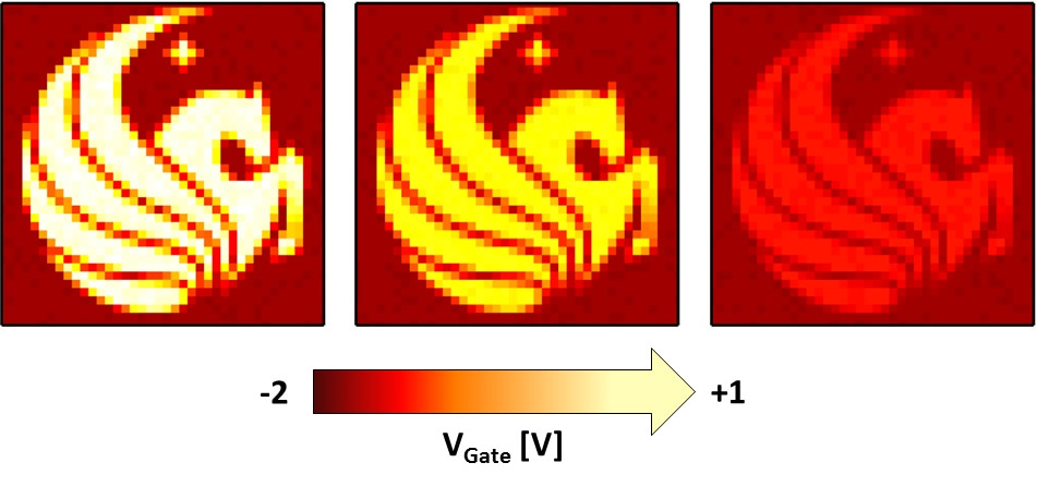
Ans: We wanted to demonstrate imaging using this novel detector – as an ultimate demonstration. However, integration of complex read-out electronics in terms of focal plane array is complicated and not easily accessible. In order to circumvent this problem, we had to device a single pixel imaging scheme where one detector element was used to scan an image plane instead to capture an IR image.
7. Anything that stroke you as particularly surprising, unexpectedly pleasant/unpleasant during the peer review process?
Ans: We are impressed by the quality of constructive review comments which helped us improve the content and clarity of the manuscript significantly. Especially, the detector noise characterization and our description of detector measurement protocol were reinforced and became more explicit.
8. Which is the development in the field of 2D materials that you would like to see in the next 10 years?
Ans: 2D materials made quite a few promises over the last decade. However, nothing tangible is developed, yet. I expect a real, practical application based on a 2D material in the next decade to address or solve a critical need which a traditional 3D material cannot fulfill.
9. And now, what’s next?
Ans: We will continue to improve the performance of the detector. An uncooled LWIR detection and imaging system is critically important for multiple applications. In parallel we have started working with commercial companies for electronic integration and hope to make it a real product someday soon.
Follow the Topic
-
Nature Communications
An open access, multidisciplinary journal dedicated to publishing high-quality research in all areas of the biological, health, physical, chemical and Earth sciences.
Related Collections
With Collections, you can get published faster and increase your visibility.
Women's Health
Publishing Model: Hybrid
Deadline: Ongoing
Biosensing
Publishing Model: Hybrid
Deadline: Jun 30, 2026


Please sign in or register for FREE
If you are a registered user on Research Communities by Springer Nature, please sign in
Wonderful contribution and flatchat :-)