Lead Telluride: well known, often used, but not completely understood
Published in Electrical & Electronic Engineering

Harald Böttner, Paul Simon
It is like in normal life: if somebody or something does hide or mask the intrinsic truth the interest will usually increase until all secrets are disclosed. The same holds for the scientific field of semiconductors. Here, the special feature is characterised by the fact that exclusively the basic necessity “to be not perfect” causes the multiple use. Semiconductors are billion sellers. As a matter of course, we are familiar with computers, mobile phones and we are astonished about the results of deep space research. These and numberless other applications are possible due to steadily increasing deeper basic knowledge of the atomistic processes behind the imperfect nature of the semiconductors. Here. we will elucidate the atomistic explanation of a long-time mysterious behaviour of a semiconductor, which was used for IR-lasers, IR-detectors and most prominent in the field of thermoelectrics. In the area of thermoelectrics, the semiconductor lead telluride (PbTe) is the mostly used material to convert thermal energy into electrical energy at elevated temperatures. It is obvious that generally such a material could play an important role to use the ecologically worthwhile, but otherwise rejected heat. By the way, it should be mentioned that PbTe was the concealed star, hardly ever mentioned as crucial for the power supply of some famous NASA launches in the 1970ies [1].
Nevertheless, this material was used with success up to now, although its metal-to-semiconductor transition with increasing temperatures was not clarified. Every attempt to clarify this crossover assumes that the simple cubic NaCl-type crystal structure of PbTe remains basically unchanged. Re-solution of Te in the PbTe-matrix after single crystal growth by the Bridgman technique, and also vaporization of the volatile Te had been discussed [2,3]. Also, impacts on the band model were considered [4,5]. A strong hint, that structural disorder could be the reason for this transition, was the observation that unusual anisotropic peaks in the XRD pattern disappear temperature dependent in correlation with the metal-to-semiconductor transition. The best key to resolve possible changes in structural disorder on the atomistic scale was the use of in-situ TEM techniques applied to samples prepared from a “Bridgeman” p-type single crystal of lead telluride [6].
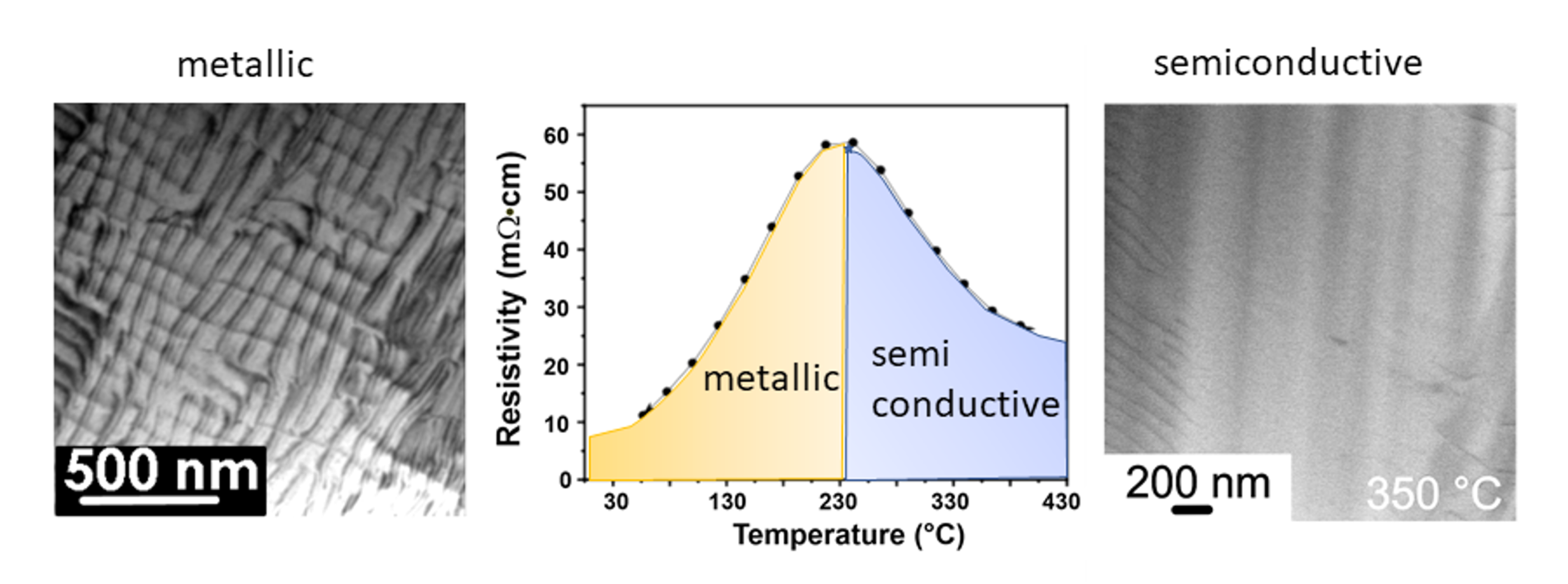
One of the decisive findings was the formation of a dislocation network due to shifts of the NaCl-like atomic slabs perpendicular to {100} below the transition temperature at 230 °C, in accordance to the occurrence of unusual anisotropic peaks in the XRD pattern mentioned above. This local structure modification on the atomistic scale causes the change in the characteristic electrical behaviour due to the appearance of in-gap electronic states with the final effect of closing the band gap of PbTe. Consequently, this results in the metal-like electronic transport behaviour at rather low temperatures. The dislocation network disappears with increasing temperature, yielding semiconductor-like electrical conductivity [Fig.1], and re-appears after cooling to room temperature restoring the metal-like behaviour. That means that cycling is not a major issue as the metal-to-semiconductor transition persists as typical feature of PbTe.

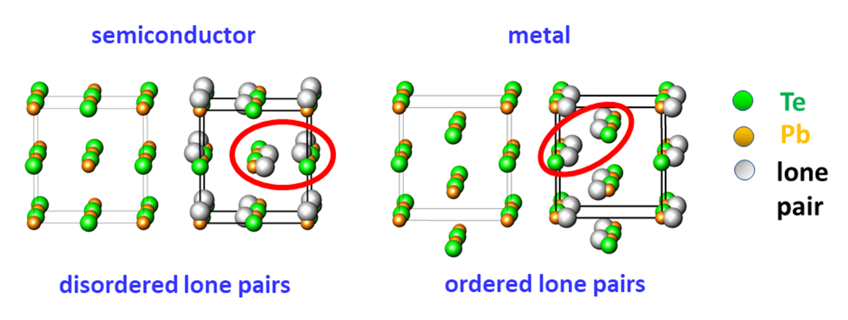
The shifts of atomic slabs perpendicular to {100} are caused by ordering of the stereochemically active lone- pairs on lead atoms below the characteristic value of 230 °C [Fig.2]. This causes changes in the electronic structure. The gap in the band structure of the ideal PbTe rock salt-type structure closes, and the material behaves like a metal in electrical transport measurements. Temperature increase above the characteristic value leads to a lone-pair disorder, and the crystal structure recovers the NaCl lattice and becomes semiconducting.

It is now nearly 70 years since the first attempts were published to explain the metal-to-semiconductor transition for PbTe and more than 50 years are passed by, that this material was of decisive importance for space research. Finally, the consequent and sophisticated use of techniques down to atomistic resolution was the key point for the last step to unravel the metal-to-semiconductor transition mystery of PbTe.
[1] Atomic power in space, a history. U.S. Department of Energy (1987), https://fas.org/nuke/space/history.pdf.
[2] Kovalchik, T. L., Maslakovets, I. P. Effect of impurities on the electrical properties of lead telluride. Sov. Physics-Technical Phys. 1, 2337-2349 (1956).
[3] Smith, R. A. The electronic and optical properties of the lead sulphide group of semi-conductors. Physica 20, 910-929 (1954).
[4] Crocker, A. J., Rogers, L. M. Interpretation of the Hall coefficient, electrical resistivity and Seebeck coefficient of p-type lead telluride. Br. J. Appl. Phys. 18, 563-573 (1967).
[5] He, J.-A., Xia, Y., Naghavi, S. S., Ozoliņš, V., Wolverton, C. Designing chemical analogs to PbTe with intrinsic high band degeneracy and low lattice thermal conductivity. Nature Comm. 10, 719-727 (2019).
[6] Gille, P., Mühlberg, M., Parthier, L., Rudolph, P. Crystal growth of PbTe and (Pb,Sn)Te by the Bridgman method and by THM. Cryst. Res. Technol. 19, 881-891 (1984).
Original article
Zelenina, I., Simon, P., Veremchuk, I. et al. Structural complexity and the metal-to-semiconductor transition in lead telluride. Commun Mater 2, 99 (2021).
https://doi.org/10.1038/s43246-021-00201-7
https://www.nature.com/articles/s43246-021-00201-7
Harald Böttner, harald.boettner@gmx.de
Paul Simon, Paul.Simon@cpfs.mpg.de
Follow the Topic
-
Communications Materials
A selective open access journal from Nature Portfolio publishing high-quality research, reviews and commentary in all areas of materials science.
Related Collections
With Collections, you can get published faster and increase your visibility.
Materials for quantum sensing and computing
Publishing Model: Open Access
Deadline: Jul 09, 2026
Triboelectric nanogenerators for energy harvesting
Publishing Model: Open Access
Deadline: Jun 30, 2026


Please sign in or register for FREE
If you are a registered user on Research Communities by Springer Nature, please sign in