Mapping of the mechanical response in Si/SiGe nanosheet device geometries
Published in Electrical & Electronic Engineering
For decades the microelectronic industry has been able to maintain an exponential scaling of device size, known as Moore’s law, roughly doubling circuit density every generation due in large part to the ingenuity and resourcefulness of scientists and engineers. However, challenges to the gains that can be achieved by simple lithographic scaling is no longer sufficient to keep up with the demands of high-performance computing applications. We have employed new materials and new ways of computing to maintain this cadence, partly because not all aspects of device behavior have been able to scale due to fundamental limitations of the constituent structures. For example, the incorporation of heteroepitaxial materials, such as silicon-germanium alloys, deposited in the vicinity of the channel regions of silicon-based devices has been utilized in several technology nodes to induce strain and improve carrier mobility.
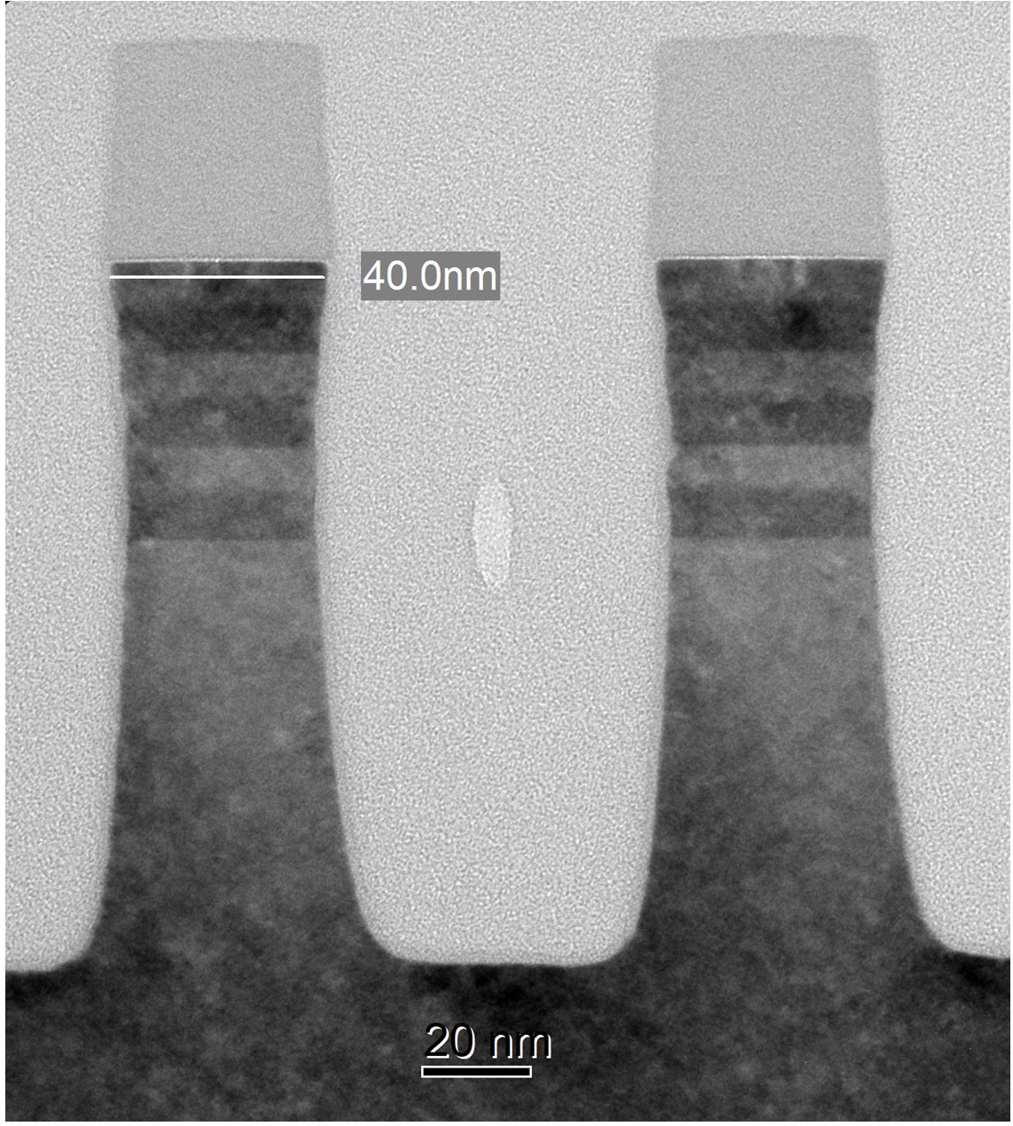
Another example has been the evolution from planar technologies to three-dimensional transistor architectures, such as FinFET’s, because the ability to control the threshold characteristics becomes more difficult as channel regions get smaller. The structures we investigated, as detailed in our manuscript, “Mapping of the mechanical response in Si / SiGe nanosheet device geometries” (https://www.nature.com/articles/s44172-022-00011-w) involve the study of nanosheets, the next generation of devices beyond FinFET’s to address the performance needs below the 7 nm technology node. By stacking fins vertically and employing a gate-all-around geometry, better device control can be achieved. However, experimentally verifying the strain states within these structures is critical due to their greater flexibility. At the same time, device scaling has also led to the issue of testing or surpassing the limits associated with the spatial resolution of many characterization techniques at our disposal. In fact, transmission electron microscopy is often used to image our devices because it possesses the necessary lateral spatial resolution (see Figure 1). However, the corresponding sample preparation is extensive, and the process of extricating a thin sample can alter the properties of the original material. This is particularly important as we consider the more complex device geometries where preserving their environment is crucial.

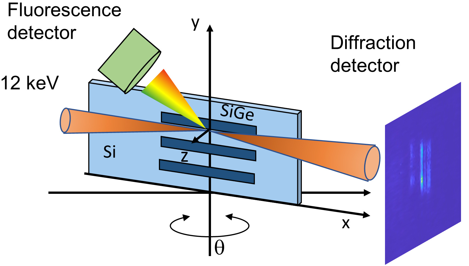
The use of synchrotron-based characterization has been integral to the efforts of IBM Research (https://research.ibm.com) since the opening of the National Synchrotron LightSource at Brookhaven National Laboratory 4 decades ago. The ability to probe the depth-dependent properties of materials non-destructively represents a key asset of such measurements. The current collaboration with scientists at NSLS-II (https://www.bnl.gov/nsls2), a state-of-the-art, third-generation synchrotron source, has enabled us to investigate a variety of structures with unprecedented brightness and resolution. At the Hard X-ray Nanobeam (HXN) beamline, by exploiting in-house developed nanofocusing multilayer Laue lense optics, the beamline scientists are able to generate a spot size of approximately 12 nm for imaging applications. Figure 2 depicts the geometry used in the reciprocal spacing mapping of Si / SiGe nanosheet structures fabricated at the IBM Albany facility, where a 12 keV photon energy was used to map deformation across a spectrum of feature widths. Distributions of lattice spacing and rotation were quantified from individual nanosheets ranging from 40 nm to 1000 nm wide.

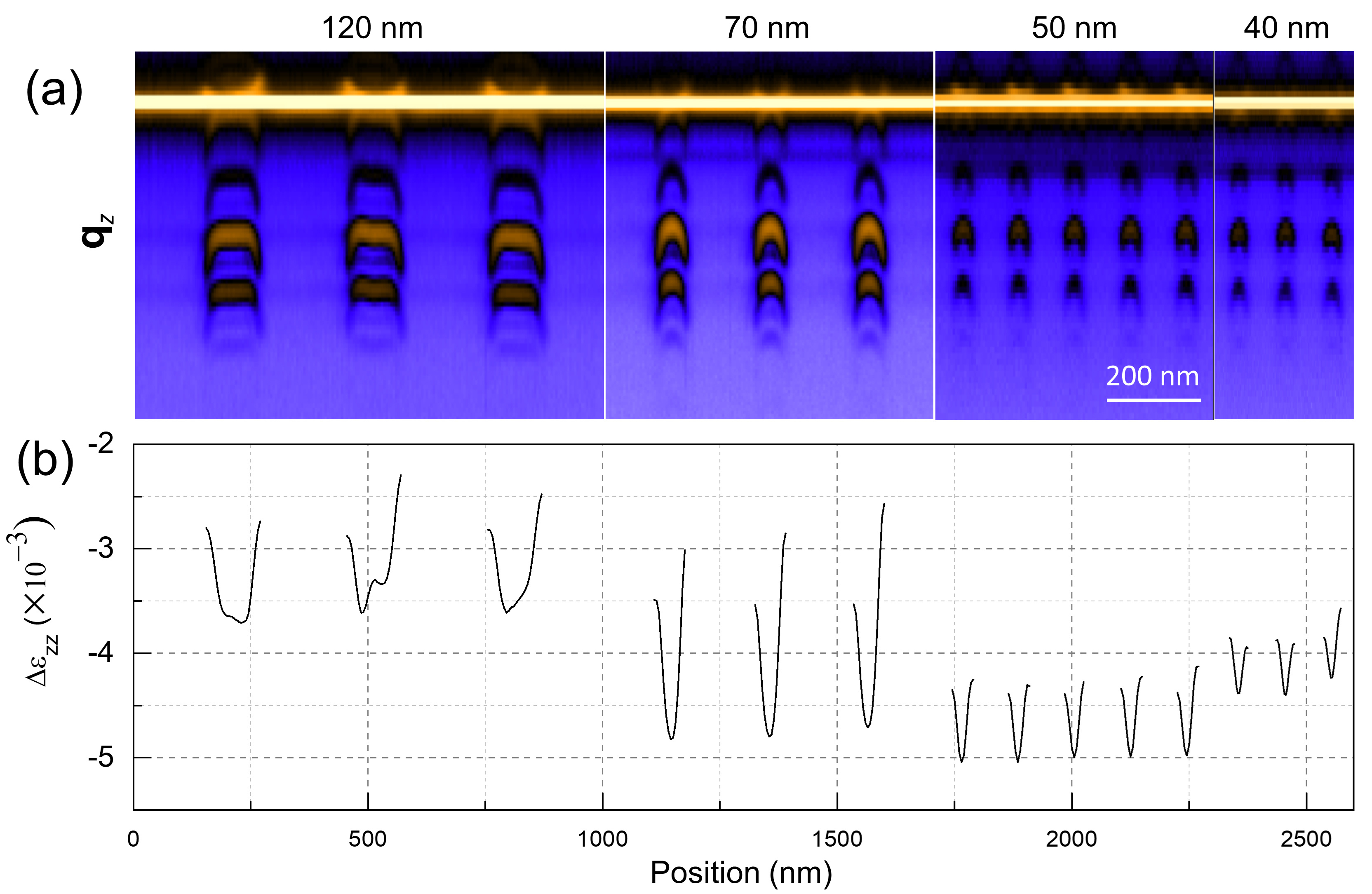
The results, as shown in Figure 3b, revealed two distinct modes of deformation within the nanosheets. As discussed in the manuscript, the first is due to elastic relaxation generated by the presence of the nanosheet’s lateral free edges, which we measured about 15 years ago (https://aip.scitation.org/doi/pdf/10.1063/1.1938277). However, these measurements allowed us to quantify a second mode induced by the interplay between the adjacent Si and SiGe layers impacting their deformation at a much finer length scale near the nanosheet edges. These trends were confirmed by computational mechanics simulations by IBM researchers, highlighting the importance of understanding both aspects of deformation at the nanoscale when predicting the carrier mobilities within current and future generation devices.

Follow the Topic
-
Communications Engineering
A selective open access journal from Nature Portfolio publishing high-quality research, reviews and commentary in all areas of engineering.
Related Collections
With Collections, you can get published faster and increase your visibility.
Engineering the future of 2D transistors: scaling, p-doping, and contact strategies
Publishing Model: Open Access
Deadline: May 31, 2026
Microgrids and Distributed Energy Systems
Publishing Model: Hybrid
Deadline: Jun 30, 2026


Please sign in or register for FREE
If you are a registered user on Research Communities by Springer Nature, please sign in