Unlocking 3D IC Performance: Cu-Cu Hybrid Bonding from Physical Mechanisms to System Integration

As AI accelerators, HBM, and chiplets push packaging beyond traditional interconnects, hybrid bonding enables finer pitch, lower latency, and better thermal performance. This review maps the field from physics to system deployment, offering a lens on why hybrid bonding matters now.
Unlocking 3D IC Performance: Cu-Cu Hybrid Bonding from Physical Mechanisms to System Integration
Like

Share this post

Choose a social network to share with, or copy the URL to share elsewhere

This is a representation of how your post may appear on social media. The actual post will vary between social networks

Explore the Research

Springer Nature Singapore
Springer Nature Singapore Springer Nature Singapore

Cu–Cu hybrid bonding technology: from physical mechanisms to system integration for 3D ICs - Moore and More

With the rapid development of microelectronic technology toward high-performance and high-density integration, traditional bonding methods face dual challenges of interconnection density and bonding temperature. The Cu–Cu hybrid bonding, leveraging its outstanding benefits in sub-micron interconnection and efficient thermal management, has emerged as an innovative solution to overcome the limitations of traditional packaging. This paper systematically explores the physical mechanisms, integration technologies, key process breakthroughs, and macroscopic applications of Cu–Cu hybrid bonding. The study highlights the revolutionary advantages of hybrid bonding, such as ultra-fine vertical interconnection spacing. A detailed analysis of two major physical mechanisms in key technical pathways is presented. In practical applications, Cu–Cu hybrid bonding has demonstrated success in high-bandwidth memory, three-dimensional heterogeneous integration, and complementary metal–oxide–semiconductor image sensors. A notable example is Sony’s Cu/SiO₂-bonded image sensor, markedly improving imaging quality and integration density. However, challenges such as thermal boundary resistance control, process complexity, and large-scale production costs remain barriers to industrialization. Future advancements, including novel passivation materials and integration with ultra-wide bandgap semiconductors, promise to further propel the performance and reliability of radio frequency (RF) devices, power electronics, and artificial intelligence chips. This review provides a comprehensive framework for both theoretical exploration and practical implementation of Cu–Cu hybrid bonding technology.

Key Technical Highlights

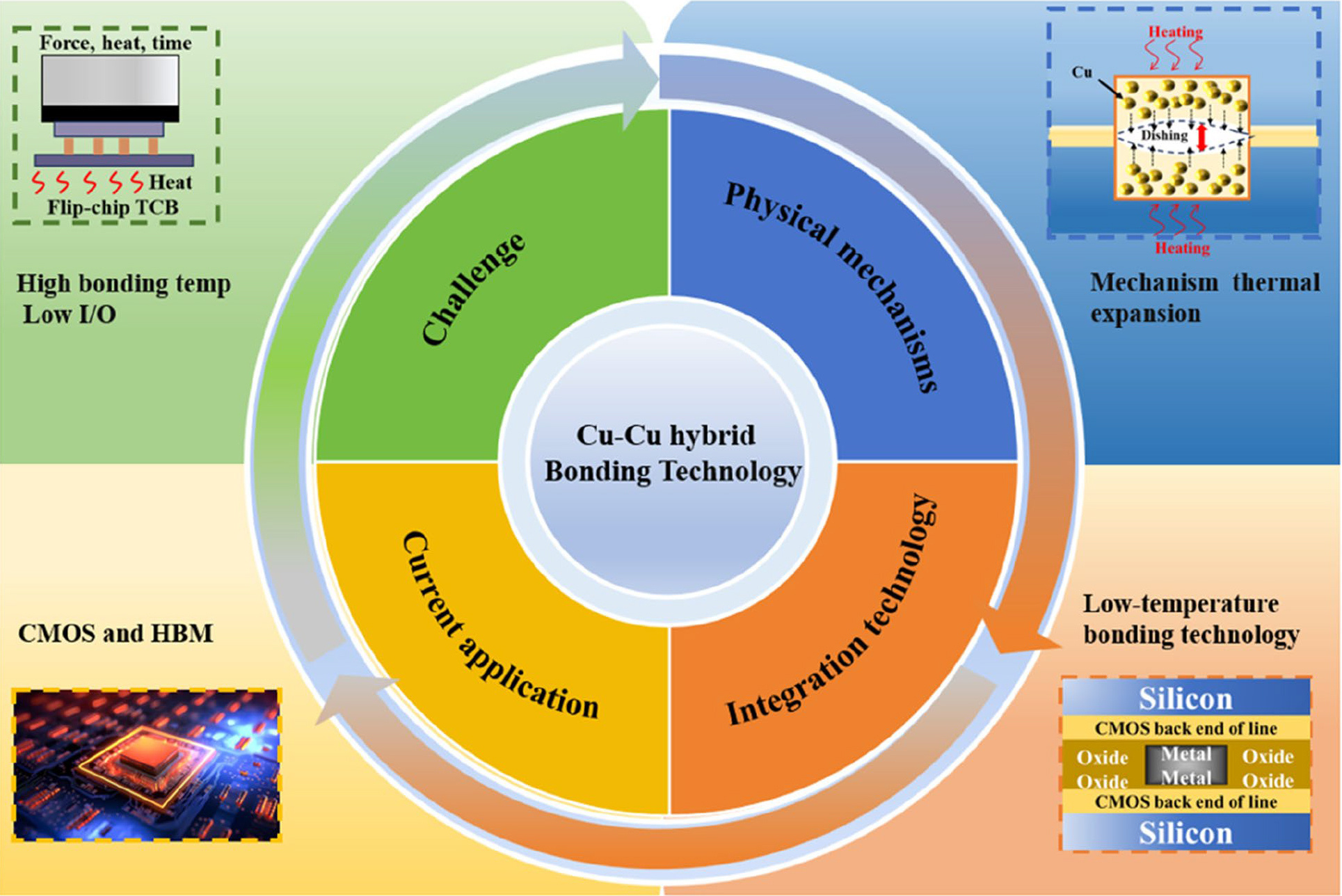
  • Why it matters: Cu-Cu hybrid bonding offers ultra-fine vertical interconnect spacing, strong electrical and thermal conductivity, and a clear path beyond conventional bump-based packaging.
  • Core mechanisms: The review explains both DBI-style oxide-assisted hybrid bonding and surface-activated bonding, showing how hydrophilic dielectric interfaces and copper diffusion jointly determine bond quality.
  • Low-temperature progress: Passivation layers such as Ru, Pd, Ag, and Ti are helping reduce bonding temperature while suppressing oxidation and preserving interface reliability.
  • Manufacturing levers: Surface planarity, CMP optimization, dielectric cleanliness, annealing control, and stress management remain decisive factors for yield and reproducibility.
  • Where it is already working: The technology is advancing HBM stacking, 3D chip integration, CMOS image sensors, and GaN/Si heterogeneous integration for high-performance electronics.

Technological Implications

The review also makes the industrial picture clear: hybrid bonding is no longer just a lab concept. It is already shaping memory, imaging, advanced packaging, and next-generation power/RF systems. At the same time, challenges such as thermal boundary resistance, process complexity, alignment tolerance, and cost-efficient mass production still define the frontier.

Challenges and Future Directions

Looking ahead, the strongest opportunities lie in low-temperature bonding, higher integration density, and broader use in AI chips, HBM, and heterogeneous semiconductor platforms. For researchers and engineers working on advanced packaging, this paper provides a compact framework for connecting materials science, process engineering, and system-level design.

Toward the Future of 3D Integration

Cu-Cu hybrid bonding is rapidly evolving into a cornerstone technology for next-generation microelectronics—bridging the gap between device-level innovation and scalable 3D system integration.

Please sign in or register for FREE

If you are a registered user on Research Communities by Springer Nature, please sign in

Follow the Topic

Electronics and Microelectronics, Instrumentation
Technology and Engineering > Electrical and Electronic Engineering > Electronics and Microelectronics, Instrumentation
Engineering and Technology Education
Humanities and Social Sciences > Education > Professional and Vocational Education > Engineering and Technology Education
Electronic Circuits and Systems
Technology and Engineering > Electrical and Electronic Engineering > Electronic Circuits and Systems

Related Collections

With Collections, you can get published faster and increase your visibility.

Emerging memory technology

The problem of memory wall between fast processors and relatively slow memory has become a critical bottleneck limiting the chip performance beyond Moore’s law. Emerging memory technologies bring new opportunities to break the memory wall for future data-intensive applications. They focus on addressing the limitations of traditional memory solutions in terms of speed, density, energy efficiency, and scalability. These technologies include but are not limited to resistive random-access memories (RRAMs), magnetoresistive RAMs (MRAMs), phase-change memories (PCMs), and ferroelectric memories. They are critical for new types of memories and in-memory computing toward the applications in AI, edge computing, and neuromorphic computing.

Publishing Model: Open Access

Deadline: Apr 30, 2026