Highly efficient large-area perovskite light-emitting diodes for next-generation display technology
Published in Electrical & Electronic Engineering
With an advent of information society, humans began to find an information in a television, computer, smartphone and etc. As the technology has advanced and the amount of information grows, display technology needs to show information more clearly and vividly. In this sense of line, display technology has focused on realizing high color purity light and natural color by finding an emitting material which can emit high color purity with narrow spectral linewidth. Inorganic quantum dots (QDs) with full width at half maximum (FWHM) ~ 30 nm have emerged as a high color purity emitter following organic emitters (FWHM > 50 nm). However, they still cannot meet the requirement of REC.2020, new color standard for ultra-high-definition television (UHD-TV), and have suffered from size-dependent color purity and wavelength. Metal halide perovskite emitters which have high color-purity (FWHM < 20 nm) and satisfy REC.2020 have great attention as a promising light emitter in future large-area solid-state lighting and displays. However, perovskite polycrystalline films, which were mostly fabricated by spincoating in high efficiency perovskite light-emitting diodes (PeLEDs), form non-uniform films in a large area and thus limit electroluminescence efficiency, reproducibility, uniformity and mass-production of large-area PeLEDs.

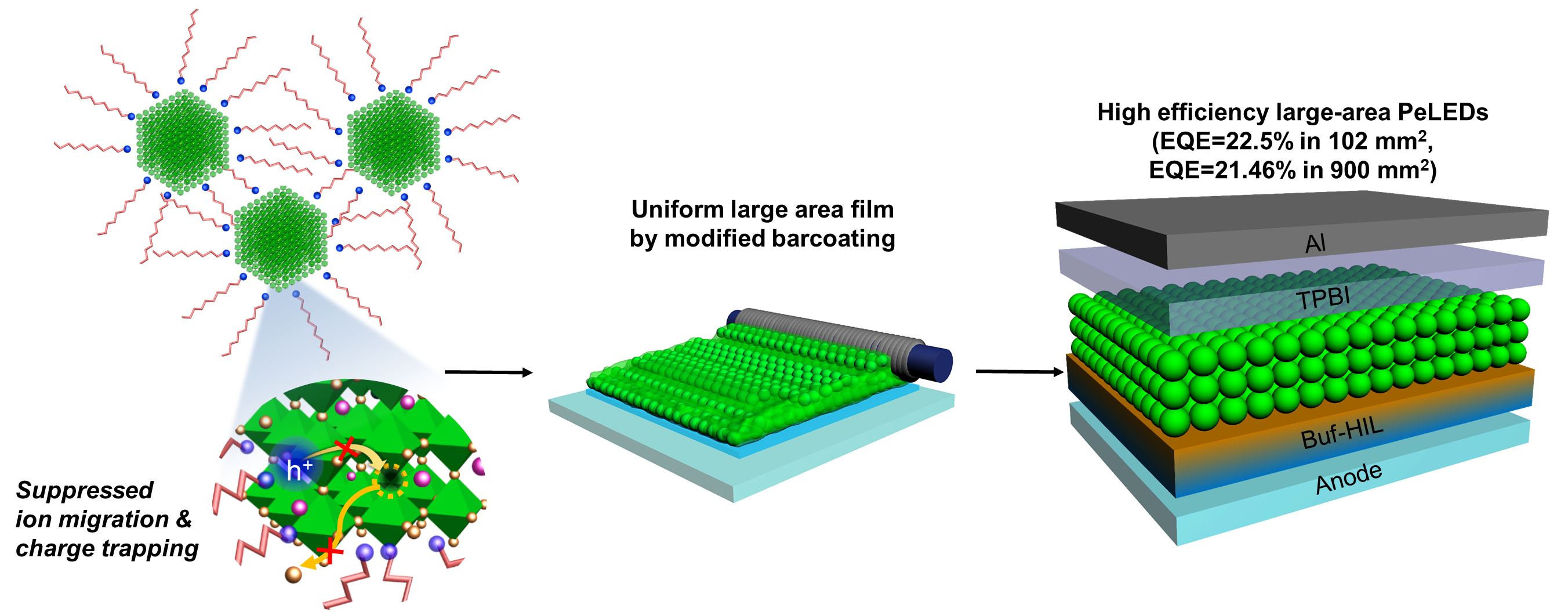
Figure 1. Schematic illustrations of full advantages of colloidal PNCs for large area barcoated PeLEDs. Schematic illustrations of suppression of charge trapping and ion migration (left), fabrication of uniform PNC films by modified barcoating (middle), and fabrication of high efficiency PeLEDs in large areas (right).
In our manuscript “Exploiting the full advantages of colloidal perovskite nanocrystals for large-area efficient light-emitting diodes” (https://doi.org/10.1038/s41565-022-01113-4), we address these concerns.
Here, we report that highly-efficient large area PeLEDs with high uniformity can be realized by the use of colloidal perovskite nanocrystals (PNCs), which decouples the crystallization of perovskites from the film formation. PNCs are pre-crystallized and surrounded by organic ligands, and thus are not affected by the film formation process, so simple modified barcoating which facilitates the evaporation of residual solvent provides uniform large-area films (Fig. 1). PeLEDs that incorporated the uniform barcoated PNC films achieved external quantum efficiency (EQE) of 23.26% in a pixel area of 4 mm2, EQE of 22.5% in 102 mm2 and EQE of 21.46% in 900 mm2, which provides a promising way toward a development of large-scale industrial displays and solid-state lighting that uses perovskite emitters.

Figure 2. Schematic illustrations of fabrication of uniform PNC films through modified barcoating.
Unlike conventional approach which uses polycrystalline bulk films that crystallize during the film formation, PNCs are pre-crystallized and solvated in non-polar solvents due to surface capping ligands. Moreover, modified barcoating induces fast solvent evaporation and forms uniform PNC films in a large area by following process (Fig. 2);
Mechanism 1) Tilting the substrate generates gravity-induced-stress on the PNC solution, which moves the PNC meniscus in the tilting direction (e.g., in the direction of gravity);
Mechanism 2) Rapid solvent evaporation occurs in front of the moving meniscus (near the contact line);
Mechanism 3) Convective flow occurs in the bulk (interior) of the droplet toward the contact line of the droplet to compensate for the rapid evaporation of the solvent;
Mechanism 4) PNCs are transported from the bulk (interior) of the droplet toward the contact line of the droplet along with convective flow and then densely packed and ordered in front of the meniscus;
Mechanism 5) PNCs are assembled on contact line edge of the meniscus by attractive capillary forces between moving meniscus and under layer, which forms uniform PNC films.
Furthermore, in PNC films, surface capping organic ligands effectively suppress the ion-migration and charge-trapping during the operation of PeLEDs, which are confirmed by low capacitance at low frequency, increased activation energy for ion migration, magnetic field-independent photoluminescence and no overshoot in transient electroluminescence. PeLEDs based on modified-barcoated formamidinium (FA) lead bromide (FAPbBr3) PNCs achieved current efficiency of 71 cd A-1 and external quantum efficiency (EQE) of 15.4% while PeLEDs based on modified-barcoated FAPbBr3 polycrystalline bulk films showed very low current efficiency of 0.0000676 cd A-1.
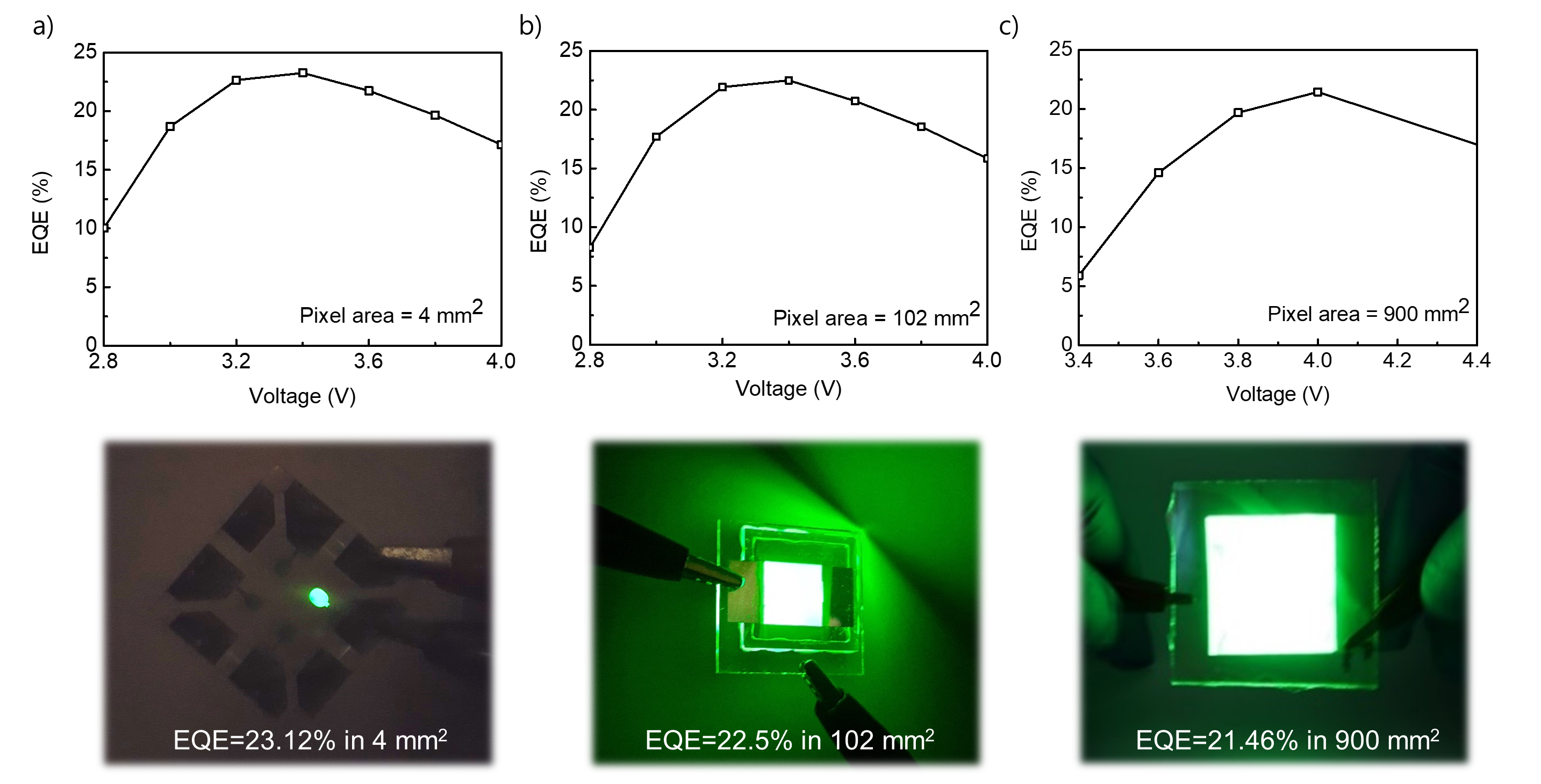
To further increase the electroluminescence efficiency of PeLEDs based on modified-barcoated PNCs, we additionally added ~ 12.5 % molar ratio of guanidinium (GA) into FAPbBr3 PNCs and overcoated 1,3,5-tris(bromomethyl)-2,4,6-triethylbenzene (TBTB) interlayer on top of the FA0.875GA0.125PbBr3 PNC films. PeLEDs based on modified-barcoated FA0.875GA0.125PbBr3 PNC achieved high EQE = 23.26% in a pixel size of 4 mm2 and showed high reproducibility in 52 devices. Furthermore, modified-barcoated FA0.875GA0.125PbBr3 PNC based PeLEDs maintained high EQE = 22.5 % in a large pixel area of 102 mm2 with a high reproducibility in 20 devices and EQE = 21.46% in a pixel area of 900 mm2.

Figure 3. Characteristics of PeLEDs. a, External quantum efficiency (EQE) (top) and photograph of operating devices (bottom) of PeLEDs with a pixel area of 4 mm2. b, EQE (top) and photograph of operating devices (bottom) of PeLEDs with a pixel area of 102 mm2. c, EQE (top) and photograph of operating devices (bottom) of PeLEDs with a pixel area of 900 mm2.
To the best of our knowledge, this result is the first demonstration of PeLEDs that use printed PNC films and shows significant improvement compared to the previously reported large-area PeLEDs based on perovskite polycrystalline bulk films (EQE = 12.7% in 100 mm2 [1], EQE = 12.1% in 900 mm2 [2], EQE = 16.4% in 900 mm2 [3]). This method suggests a step toward the development of perovskite emitters in industrial displays and solid-state lighting.
[1] Chu, S., Chen, W., Fang, Z., Xiao, X., Liu, Y., Chen, J., Huang, J. and Xiao, Z., 2021. Large-area and efficient perovskite light-emitting diodes via low-temperature blade-coating. Nature Communications 12, p.147.
[2] Zhao, X. and Tan, Z.-K., 2020. Large-area near-infrared perovskite light-emitting diodes. Nature Photonics 14, pp.215–218.
[3] Sun, C., Jiang, Y., Cui, M, Qiao, L., Wei, J., Huang, Y., Zhang, L., He, T., Li, S., Hsu, H.-Y., Qin, C., Long, R. and Yuan M., 2021. High-performance large-area quasi-2D perovskite light-emitting diodes. Nature Communications 12, p.2207.
Follow the Topic
-
Nature Nanotechnology
An interdisciplinary journal that publishes papers of the highest quality and significance in all areas of nanoscience and nanotechnology.


Please sign in or register for FREE
If you are a registered user on Research Communities by Springer Nature, please sign in