Memristive circuits based on multilayer hexagonal boron nitride for radiofrequency and millimetre wave applications
Radiofrequency (RF) data transmission switches for millimetre wave (mmWave) applications are a fundamental building block in modern wireless transceivers covering 5G and 6G communication bands1. The concept of their functionality is rather straightforward: they switch between (i) blocking a high-frequency signal from different sections of a circuit (isolation), and (ii) transmitting it with the least power loss possible. As simple as this may sound, it is actually very challenging, particularly as wideband communication standards are being pushed to higher frequencies (beyond hundreds of GHz) in order to improve data rates for applications such as augmented and virtual reality and the Internet-of-Things1.
At such high frequencies, non-idealities, device parasitics, and performance need to be carefully considered to achieve acceptable performance metrics. Different technologies target these needs in integrated circuits, like micro-electro-mechanical systems (MEMS), semiconductor devices (transistors, diodes and varactors) and, more recently, memristors based on phase-change or metal-insulator transition materials1. Each technology shows its own upsides, but operation beyond tens of GHz is hard to achieve.
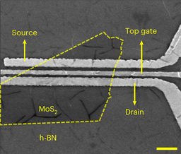
Memristors are relatively simple structures, sandwiching an insulating or semiconducting layer between metal electrodes (namely, a capacitor), and capable of persistently switching their electrical resistance through electrical stimuli. Memristors made of single-layer 2D materials — such as hexagonal boron nitride (h-BN) or molybdenum disulfide (MoS2) — have been explored for use as RF switches2,3. In these devices, a conductive metallic filament is formed and disrupted when controlled stress is applied, achieving operating frequencies up to 480 GHz, thanks to a very low resistance in their ON state of ~1.4 Ω (Ref. 2). However, the main problem of these RF switches is the limited endurance and unclear yield, device-to-device and cycle- to-cycle variability. The simple series switch architecture typically studied also has limited applicability.
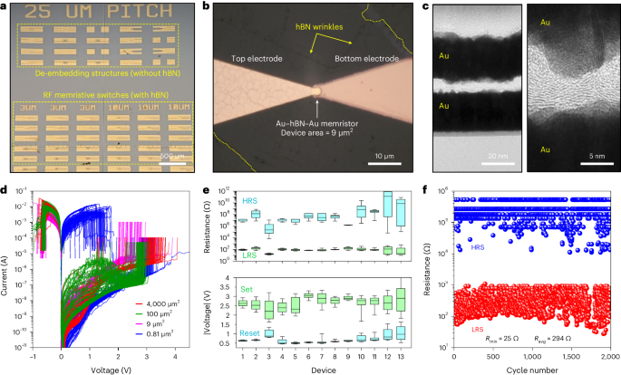
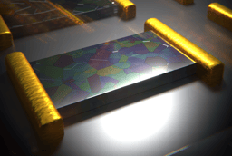
To sort out the endurance and variability issue, we thought of using multilayered h-BN (instead of monolayer) with which we have experienced a higher yield of memristors in the past4. Therefore, we fabricated large arrays of metal/h-BN/metal memristors laid-out on a RF waveguide structure that allows characterizing the devices at high frequencies5. Effectively, most devices where able to switch, with a very high yield! Moreover, using pulsed switching conditions instead of typical DC signal stress, we reached a largely improved endurance above 2000 cycles, ~66 times higher than previous reports. But the electrical performance wasn’t enough for their application as RF switches: variability was still high and the obtained resistance values in the ON condition of the switch were too large. But considering that the conduction is due to a metallic filament, we thought that better performance was possible: the device just needed to be operated in an appropriate regime to reach it.
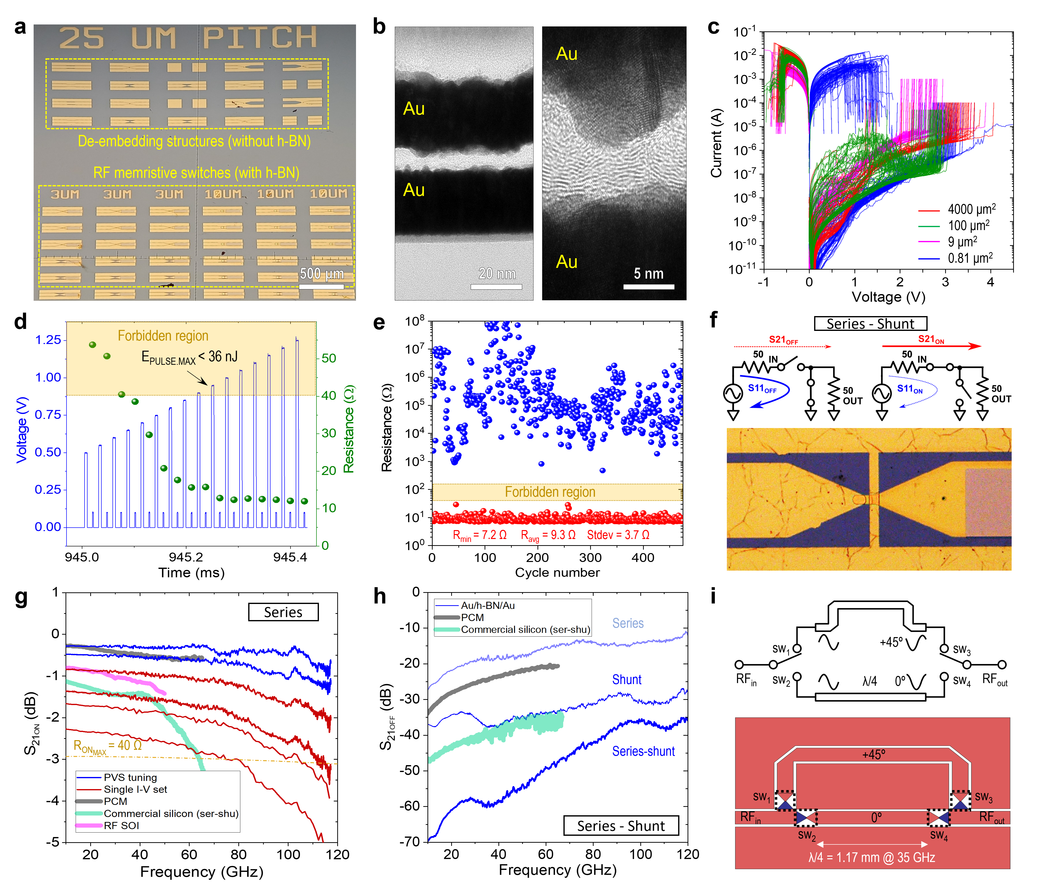
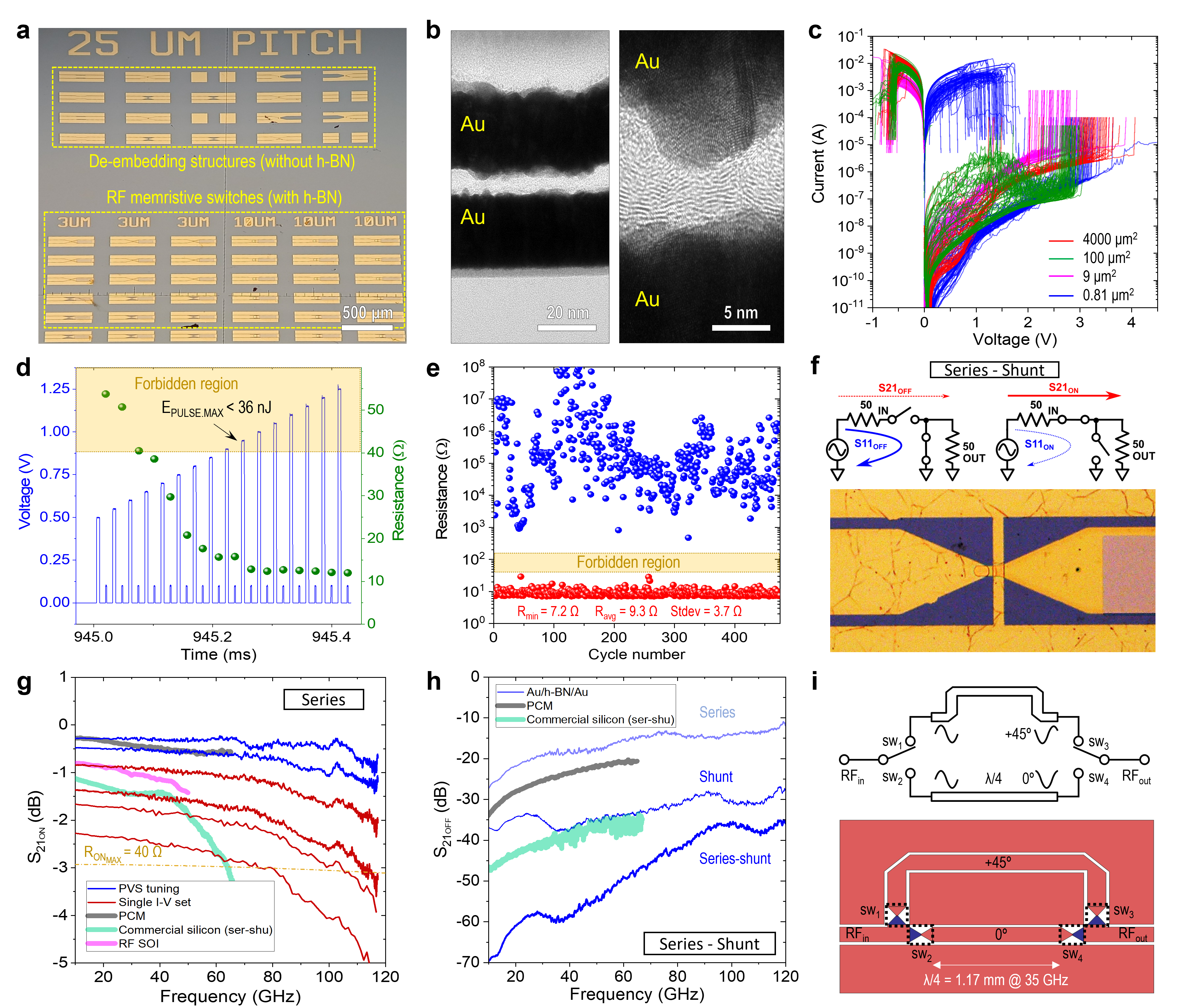
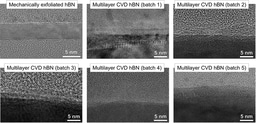
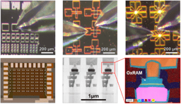
Figure 1: a, Optical microscope image of a meta/h-BN/metal array and RF de-embedding structures. b, Cross-sectional TEM images of a Au/CVD h-BN/Au device, showing layered structure. c, Characteristic I-V curves displaying at least 100 consecutive cycles for each device area. d, Conductance-enhancing protocol using 10 μs voltage pulses. e, Variability resistance through 475 cycles of a single device switched following the protocol from d. f, Circuit schematic and optical microscope image of a series-shunt Au/h-BN/Au device. g, Comparison of losses (S21.ON) between conductance-optimized Au/h-BN/Au devices, non-optimized devices and other switching technologies. h, Isolation enhancement (better than 35 dB up to 120 GHz) with series-shunt Au/h-BN/Au. i, Schematic and layout of the evaluated phase-shifter as potential use-case.
We used a conductance-enhancing method that applies short, controlled bursts of stress to the memristor. This is similar to write-verify procedures, an approach used in memristor-based artificial neural networks6 to tune the effective memristor resistance. This way, we systematically achieve ON-state resistances below 10 Ω (as low as 4.5 Ω), consistently across multiple devices, and throughout hundreds of switching cycles. When testing a single device as an RF switch, these characteristics result in very low losses (below 2 dB) and high isolation (above 30 dB) at frequencies up to 260 GHz. But the single, series-switch device is rarely employed in real RF applications, and different configurations of multiple devices are typically necessary. Therefore, we constructed RF-switch circuits with h-BN-based memristors and achieved >35 dB isolation in series-shunt configurations at 120 GHz, at least twice the frequency reported in switch technologies for integrated circuits.
After numerous experiments, including RF measurements with in-situ memristor switching, we had enough data to reliably address the applicability of our memristor RF-switch circuits. Phase shifters are key structures in modern beam-forming antenna arrays. Using the experimental RF data of multiple metal/h-BN/metal switches, we tested the performance of a phase shifter by combining electrical measurements with a full-electromagnetic wave solver. While working at 35 GHz, our memristors can vastly improve the performance of the same phase-shifter based on commercial technologies, like silicon transistor switches.
Some key upsides of these metal/h-BN/metal memristors is that they are fabricated using scalable processes (chemical vapour deposition), are wafer-scale compatible, and can be integrated into the back-end-of-line of mature silicon microchips7. Moreover, our devices operate non-polarly, which means that they can be switched using either positive or negative voltages only, greatly simplifying their integration from the circuit perspective. This overall performance owed to a combination of several areas of expertise. Reaching out to world-renowned experts in materials, memristors, and high frequency electronics, both within (Prof. Shamim) and without our own institution (Prof. Deji Akinwande, Prof. Psychogiou, Prof. de Paco, Prof. Verdú) proved fundamental to rounding device design, characterization, and application.
The promising high frequency performance of memristor RF switches in general and of our metal/h-BN/metal devices in particular can cover crucial needs in sub-THz communication bands (above 100 GHz) that current technologies struggle to meet. But the most passionate aspect to doing science is that there is always room to improve! Memristor stack optimization, h-BN quality enhancement8, electrode planarization for improved endurance, and reliable integration onto functional integrated circuits are key aspects moving forward and are great opportunities to deepen the research that will enable these devices to meet industrial requirements.
- Kim, D. et al. Emerging memory electronics for non-volatile radiofrequency switching technologies. Nat Rev Electr Eng 1, 10–23 (2024).
- Kim, M. et al. Analogue switches made from boron nitride monolayers for application in 5G and terahertz communication systems. Nature Electronics 2020 3:8 3, 479–485 (2020).
- Kim, M. et al. Monolayer molybdenum disulfide switches for 6G communication systems. Nature Electronics 2022 5:6 5, 367–373 (2022).
- Pazos, S. et al. Memristive circuits based on multilayer hexagonal boron nitride for millimetre-wave radiofrequency applications. Nature Electronics (2024), https://doi.org/10.1038/s41928-024-01192-2
- Chen, S. et al. Wafer-scale integration of two-dimensional materials in high-density memristive crossbar arrays for artificial neural networks. Nature Electronics 3, 638–645 (2020).
- Aguirre, F. et al. Hardware implementation of memristor-based artificial neural networks. Nat Commun 15, 1974 (2024).
- Zhu, K. et al. Hybrid 2D–CMOS microchips for memristive applications. Nature 618, 57–62 (2023).
- Yuan, Y. et al. On the quality of commercial chemical vapour deposited hexagonal boron nitride. Nat Commun 15, 4518 (2024).
Follow the Topic
-
Nature Electronics
This journal publishes both fundamental and applied research across all areas of electronics, from the study of novel phenomena and devices, to the design, construction and wider application of electronic circuits.

Please sign in or register for FREE
If you are a registered user on Research Communities by Springer Nature, please sign in