Yield, variability, reliability, and stability of electronic devices made of two-dimensional layered materials
Published in Electrical & Electronic Engineering
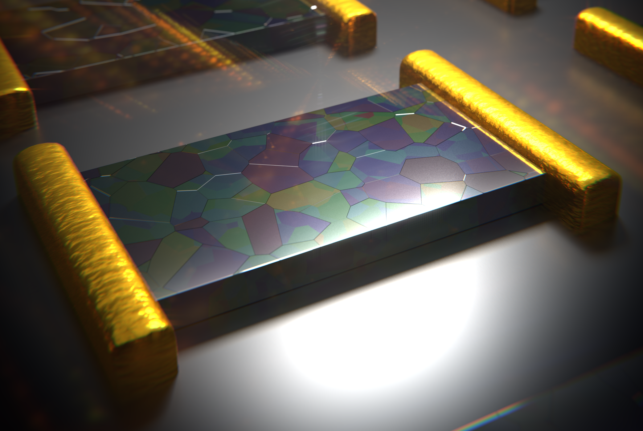
Reproducibility of scientific experiments is a big concern [1-2]. In the field of two-dimensional (2D) layered materials (LM) we have witnessed how top journals have sometimes published articles in which ground-breaking claims were supported by scarce data. In many cases, the excuse was that the materials were obtained via mechanical exfoliation of bulk crystal powder [3], which does not allow the fabrication of multiple devices in parallel and strongly difficult getting data from hundreds of 2D-LMs based structures.
Fortunately, around 2008 scalable methods to synthesize 2D-LMs were developed, being chemical vapour deposition (CVD) [4] and liquid phase exfoliation (LPE) [5] those that have raised most interest. These developments have attracted the interest of the semiconductors industry, which is hungry of novel nanomaterials and nanostructures that could extend the Moore’s law, and/or contribute to the development of devices beyond the complementary metal-oxide-semiconductor (CMOS) technology [6-7].
In the process of integrating 2D-LMs in semiconductor production lines, researchers based at universities and institutes could play an important role because they could choose to employ industry-compatible methods, and at the same time they do not have the multiple restrictions (in terms of contamination and high processing costs) that companies have. This flexible position allows them to try new materials and device configurations using CVD and LPE, which could produce important advances in this field. As an example, most state-of-the-art electronic circuits made of 2D-LMs have been developed at universities and research institutes [8-14], including circuital demonstrations of logic gates [8-9], operational amplifiers [10], crossbar arrays of memristors [11] and memtransistors [12], self-powered antennas [13] and advanced cameras [14]. The authors of some of these works have started to partner with companies to try to introduce their developments in the market [15].
However, it should be highlighted that the crystallographic structure of 2D-LMs synthesized using state-of-the-art scalable methods (i.e. CVD, LPE) still contains too many defects (e.g. lattice distortions, impurities, grain boundaries, dangling bonds at the junctions), which increases the inhomogeneities in the 2D-LMs sheet/film [16]. Therefore, it is extremely important that studies using CVD and LPE to synthesize 2D-LMs for electronic devices and circuits include abundant information about yield, variability, reliability and stability of the main parameters and figures-of-merit.
In our Comment article, recently published in Nature Communications [17], we clearly detail the most important considerations to take into account in this direction. All advices given have been supervised by colleagues working in the industry, and following them should increase the quality of journal papers and accelerate the introduction of 2D-LMs in electronic devices and circuits, with the consequent benefit for our society.
References
[1] Vaux, D. L. Know when your numbers are significant, Nature 492, 180–181(2012).
[2] Frommlet, F. Improving reproducibility in animal research, Scientific Reports 10, 19239 (2020).
[3] Novoselov, K. et al. Two dimensional atomic crystals. Proc. Nat. Acad. Sci. 102, 10451-10453 (2005).
[4] Li, X. et al. Large-Area Synthesis of High-Quality and Uniform Graphene Films on Copper Foils. Science 324, 1312-1314 (2009).
[5] Hernandez, Y. et al. Production of Graphene by Liquid-Phase Exfoliation of Graphite. Nat. Nanotechnol. 2008, 3, 563−568.
[6] Akinwande, D. et al. Graphene and two-dimensional materials for silicon technology. Nature 573, 507–518 (2019).
[7] Li, M.-Y. et al. How 2D semiconductors could extend Moore’s law. Nature 567, 169–170 (2019).
[8] Lin, S. et al. Solution-processable 2D semiconductors for highperformance large-area electronics. Nature 562, 254–258 (2018).
[9] Li, N. et al. Large-scale flexible and transparent electronics based on monolayer molybdenum disulfide field-effect transistors. Nat. Electron. 3, 711-717 (2020).
[10] Polyushkin, D. K. et al. Analogue two-dimensional semiconductor electronics. Nat. Electron. 3, 486–491 (2020).
[11] Chen, S. et al. Wafer-scale integration of two-dimensional materials in high-density memristive crossbar arrays for artificial neural networks. Nat. Electron. 3, 638-645 (2020).
[12] Lee, H.-S. et al. Dual-Gated MoS2 Memtransistor Crossbar Array. Adv. Funct. Mater. 2003683 (2020).
[13] Zhang, X. et al. Two-dimensional MoS2-enabled flexible rectenna for Wi-Fi-band wireless energy harvesting. Nature 566, 368–372 (2019).
[14] Goossens, S. et al. Broadband image sensor array based on graphene–CMOS integration. Nat. Photon. 11, 366–371 (2017).
[15] Website of the company Baijieteng Technology Corporation, http://bjtiot.com/english/ (accessed on November 24th 2020).
[16] Shi, Y. et al. Electronic synapses made of layered two-dimensional materials. Nat. Electron. 1, 458–465, (2018).
[17] Lanza, M., Smets, Q., Huyghebaert, C., Li, L.-J. Yield, variability, reliability, and stability of two-dimensional materials based solid-state electronic devices, Nat. Comm. 11, 5689 (2020).
Follow the Topic
-
Nature Communications
An open access, multidisciplinary journal dedicated to publishing high-quality research in all areas of the biological, health, physical, chemical and Earth sciences.
Related Collections
With Collections, you can get published faster and increase your visibility.
Women's Health
Publishing Model: Hybrid
Deadline: Ongoing
Biosensing
Publishing Model: Hybrid
Deadline: Jun 30, 2026


Please sign in or register for FREE
If you are a registered user on Research Communities by Springer Nature, please sign in