The gap between academia and industry in resistive switching research
Published in Electrical & Electronic Engineering
Today, state-of-the-art resistive switching (RS) memories offer low switching energies (around 0.1 pJ per state transition), short switching times (around 10 ns), high endurances (around 1015 cycles), and long data retention times (more than 10 years). And in 2021, standalone resistive switching memories had a global market of US$666 million. This represents around 0.4% of the total standalone memory market, and is expected to increase to around US$2.63 billion by 2027.
As well as being sold as standalone chips, resistive switching memories are being embedded in small application-specific integrated circuits (ASICs) and systems on chips (SoCs) as memory for sensors and medical instruments. Accurate calculations of the embedded memory market size is more complex than the standalone memory market because it depends on the area they occupy in the microchips, which is rarely disclosed. Embedded memory market sizes are estimated based on assumptions of the average chip area occupied by a given memory technology, and are expected to grow at a compound annual growth rate of around 95% from 2021 to 2027, increasing from around US$54 million to around US$2.9 billion. Recently it has also been suggested that such devices could be used in other applications such as neuromorphic computing systems, data encryption circuits and high-frequency telecommunication switches.
But just as it seemed as though resistive switching technologies were starting to take-off, Intel began to wind down its phase-change memory plant in Utah during the second quarter of 2022, with little detail as to why. While other smaller companies — such as Micron — have made similar decisions in the past, Intel had been developing the technology for nearly a decade. The announcement came as shock to many academic researchers, who have been telling funding agencies that standalone resistive switching technologies have vast real-world potential. Does Intel’s announcement really mean that the entire field is hyped and that only minor developments will come out of it? Will other major companies working on RS devices follow and cease RS activities? Or did Intel choose the wrong approach — and can other approaches possibly succeed? In this article recently published by Nature Electronics (click here) we analyze how challenging is to put a RS prototype memory in the market, the gap existing between academia and industry in RS research, and how to make RS studies really useful from a technological point of view.
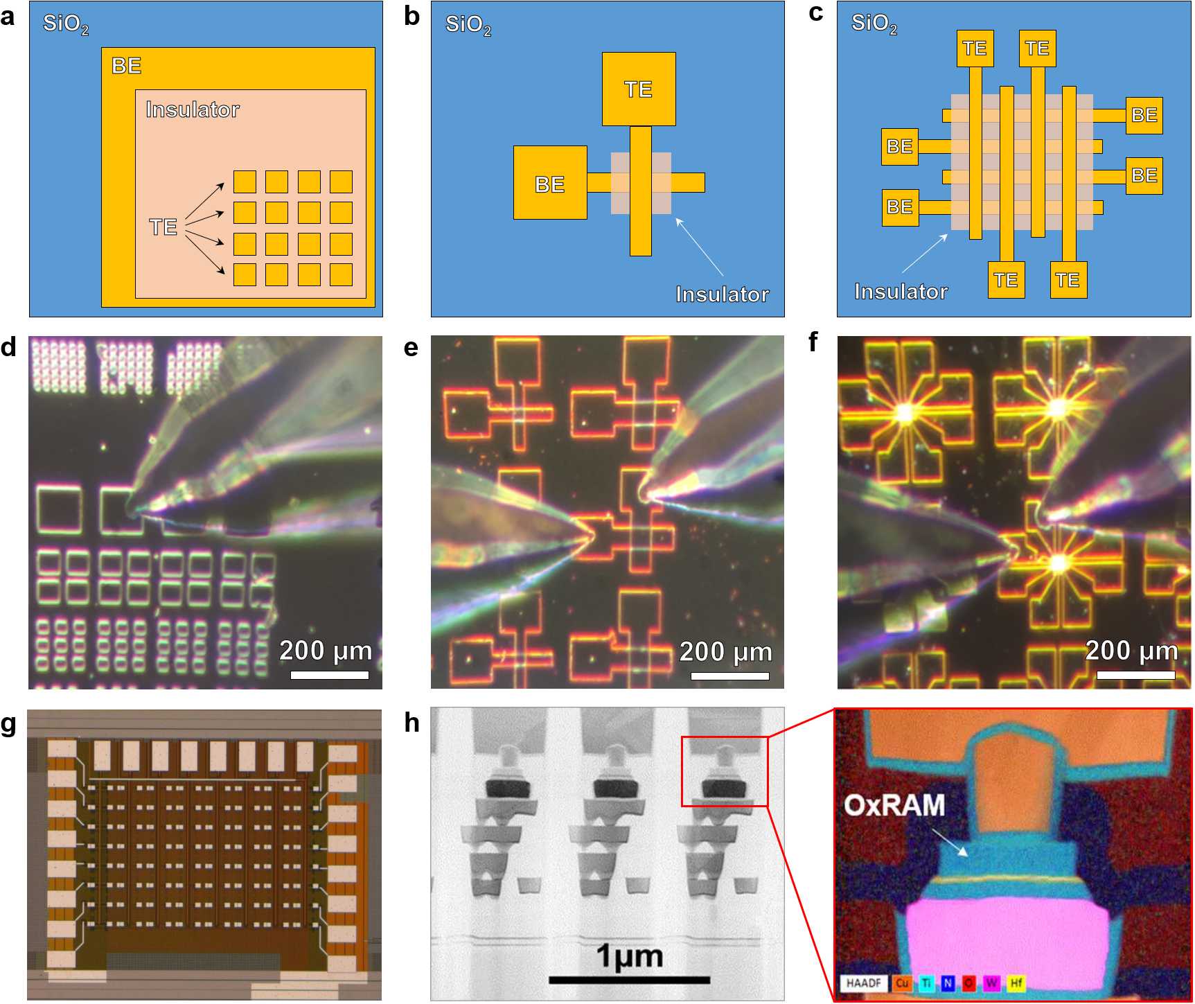
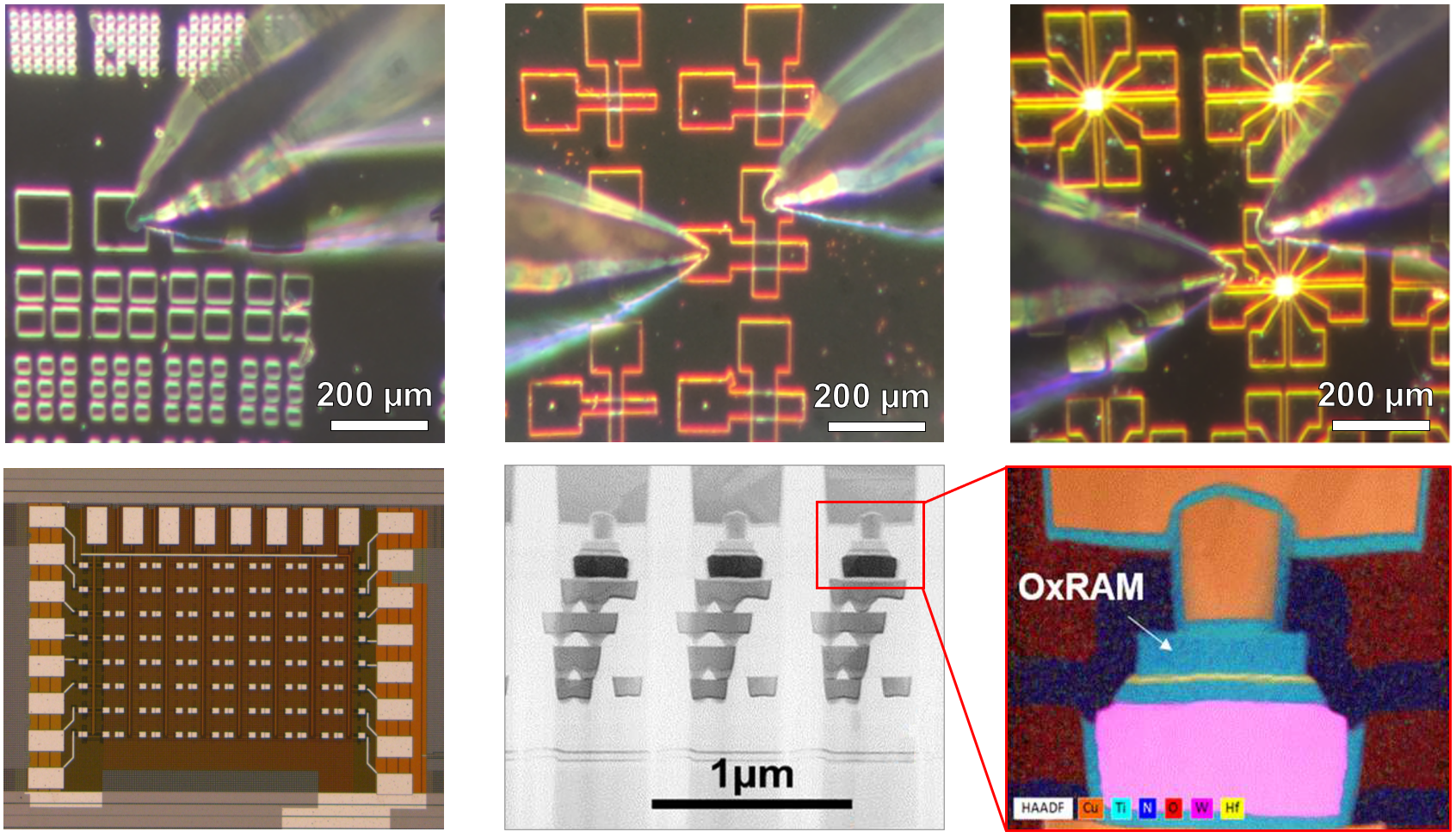
Test structures commonly used in academia and industry. a-c, Top-view schematic of three different structures often used to measure resistive switching: common bottom electrode structure, cross-point structure, crossbar structure. d-f, top-view optical microscope images of the resistive switching structures shown in a-c, with the tips contacted on the electrodes. In panel d, there is only one tip because the other electrode is the substrate of the sample. Reproduced with permission from reference [Zuo, Y. et al. Effect of the Pressure Exerted by Probe Station Tips in the Electrical Characteristics of Memristors. Advanced Electronic Materials 6, 1901226 (2020)], copyright Wiley-VCH 2020. g, Top-view optical microscope image of a part of a microchip containing a crossbar array of one-transistor-one-memristor cells. h, Cross-sectional transmission electron microscopy image of a one-transistor-one-memristor cell often employed by companies to test RS materials, which is embedded at the back-end-of-line interconnections of a microchip. The panel in the right is the energy dispersive X-ray spectroscopy image map showing the chemical composition at each single location. Adapted with permission from reference [Grenouillet, L. et al. 16 kbit 1T1R OxRAM arrays embedded in 28 nm FDSOI technology demonstrating low BER, high endurance, and compatibility with core logic transistors. IEEE International Memory Workshop (IMW), pp. 1-4 (2021)], copyright IEEE 2012.
Follow the Topic
-
Nature Electronics
This journal publishes both fundamental and applied research across all areas of electronics, from the study of novel phenomena and devices, to the design, construction and wider application of electronic circuits.


Please sign in or register for FREE
If you are a registered user on Research Communities by Springer Nature, please sign in