On the quality of commercial chemical vapour deposited hexagonal boron nitride

In recent years, the semiconductors industry has put its eyes on two-dimensional (2D) materials produced by chemical vapour deposition (CVD). This method allows synthesizing various 2D materials at the wafer scale with relatively low thickness fluctuations, paving the way for the fabrication of electronic devices and circuits [1-2]. However, commercially available CVD-grown 2D materials contain local defects, such as lattice distortions and impurities, and the density of defects increases with the thickness. A few research groups have managed to produce high-quality monolayer 2D materials via CVD [3-5] – multilayer is more complex – but their samples are not accessible to everyone. Consequently, most scientists use commercially available CVD-grown 2D materials for their studies and prototype devices.
The suppliers of CVD-grown 2D materials show on their websites materials specifications that look amazing! They show a tiny picture of the material in which perfect crystalline structure can be observed and without reporting any information about defects densities; they also give a nominal thickness without any variability ranges (neither within the same sample or from one batch to another). However, we have fabricated devices over the past five years using their CVD-grown 2D materials following an identical protocol, and the properties of the devices exhibited huge variations when we use 2D materials from different batches – although the variations within the same bath were quite low, as shown in our Nature articles [2, 6-7]. So, we have decided to explore this issue in depth.
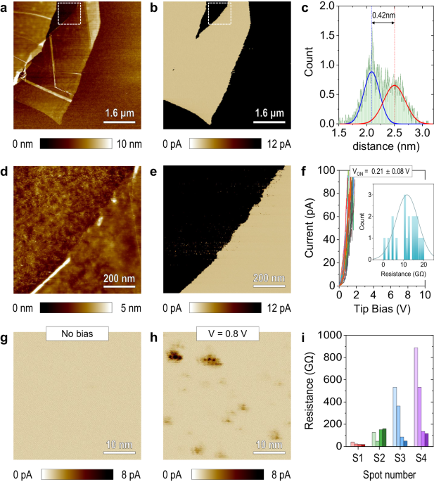
In our latest Nature Communications article [8], we have purchased monolayer and multilayer hexagonal boron nitride (hBN) from all the suppliers that we have found (in total 9) and analysed their properties using cross-sectional transmission electron microscopy (TEM), conductive atomic force microscopy (CAFM), scanning electron microscopy (SEM), and Raman spectroscopy. We also compared their properties with those of mechanically exfoliated hBN stacks with similar thicknesses. The results are simple: none of the commercially-available CVD-grown hBN samples fit the specifications indicated on the website of the manufacturer. In particular, the monolayer hBN is not such thing, it is normally around 4 to 5 layers and around 20% of its surface is highly defective or even amorphous. Their properties are very far from those of mechanically exfoliated hBN, and the monolayer CVD hBN grown by our collaborators at the King Abdullah University of Science and Technology shows much better properties. When measuring the multilayer samples, the mismatch of the properties advertised and measured are even higher, and the batch-to-batch variability is huge. Our feeling is that buying commercial CVD-grown hBN is like playing lottery: you may end up getting devices that work very well (after engineering size, electrodes, and biasing conditions), but you might have big problems to reproduce them using hBN from another batch. Please see our article for more details [8]. To be fair, we gave the suppliers the opportunity to comment (in our paper) on these differences that we observed, but several did not answer our email and only one wanted to provide one explanation (see the Final Note in our article).
Fortunately, we have started an ambitious collaboration with the world-leading manufacturer of MOCVD systems (Aixtron), which is now providing us with wafers of hBN with very good quality and, more importantly, with very small variations from one bath to another. And we see much nicer results! Hopefully combining expertise from many different institutions, we can overcome the problem of variability in 2D-materials-based devices. Kudos to the student Yue Yuan for her strong dedication to this project!

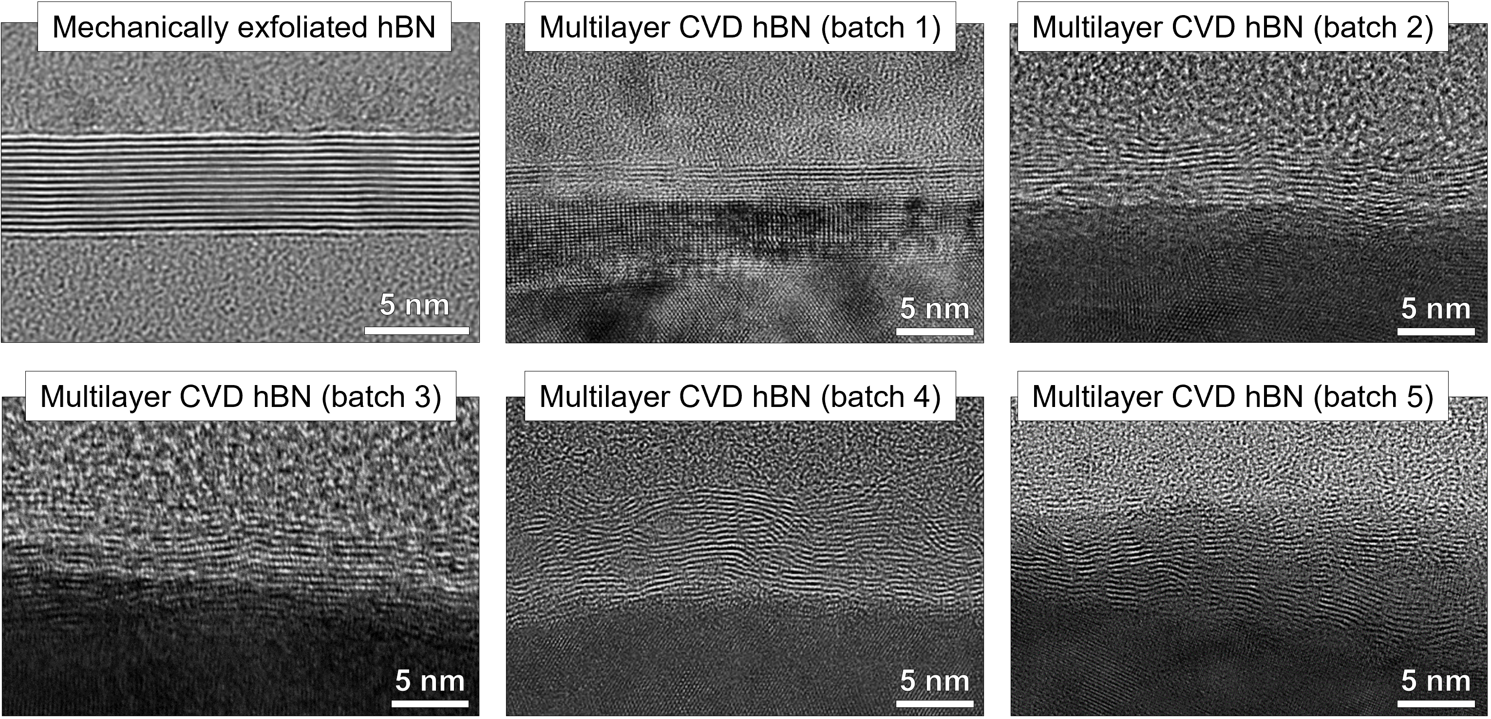
Variability in commercial CVD-grown multilayer hBN samples. High-resolution cross-sectional transmission electron microscopy (TEM) images of a mechanically exfoliated multilayer hBN sample (serving as a reference) and 5 commercial CVD-grown multilayer hBN samples from the same supplier, across 5 different batches. High variability in thickness fluctuation from batch to batch and a large defect density can be observed in the commercial CVD-grown multilayer hBN samples. The supplier indicated in its website that their multilayer hBN samples are crystalline and hold a nominal thickness of 13 nm.
References
[1] Zhu, K. et al. The development of integrated circuits based on two-dimensional materials. Nature Electronics 4, 775-785 (2021).
[2] Zhu, K. et al. Hybrid 2D/CMOS microchips for memristive applications. Nature 618, 57-62 (2023).
[3] Lin, Y. et al. Wafer-scale graphene integrated circuit. Science 332, 1294–1297 (2011)
[4] Lee, J. et al, Wafer-Scale Growth of Single-Crystal Monolayer Graphene on Reusable Hydrogen-Terminated Germanium. Science 344, 286–289 (2014).
[5] Chen, T. et al. Wafer-scale single-crystal hexagonal boron nitride monolayers on Cu (111). Nature 579, 219–223 (2020).
[6] Shi, Y. et al. Electronic synapses made of layered two-dimensional materials. Nature Electronics 1, 458-465 (2018).
[7] Chen, S. et al. Wafer-scale integration of two-dimensional materials in high-density memristive crossbar arrays for artificial neural networks. Nature Electronics 3, 638-645 (2020).
[8] Yuan, Y. et al. On the quality of commercial chemical vapour deposited hexagonal boron nitride. Nature Communications 15, 4518 (2024).
Follow the Topic
-
Nature Communications
An open access, multidisciplinary journal dedicated to publishing high-quality research in all areas of the biological, health, physical, chemical and Earth sciences.
Related Collections
With Collections, you can get published faster and increase your visibility.
Women's Health
Publishing Model: Hybrid
Deadline: Ongoing
Biosensing
Publishing Model: Hybrid
Deadline: Jun 30, 2026


Please sign in or register for FREE
If you are a registered user on Research Communities by Springer Nature, please sign in