Mid-Infrared Imaging Made Visible with Silicon

The Mid-Infrared Challenge
The mid-infrared (MIR) spectral region (2.5–25 μm), often referred to as the “molecular fingerprint region”, reveals unique vibrational features of molecules and is thus invaluable for applications in medicine, food safety, environmental sensing, and materials analysis. However, conventional MIR cameras based on narrow-bandgap materials such as HgCdTe and InSb typically suffer from high noise at room temperature and require cryogenic cooling. Silicon detectors, in contrast, perform excellently at room temperature but cannot directly detect MIR signals.
To address this challenge, researchers have exploited the principle of non-degenerate two-photon absorption (ND-2PA): an MIR photon and a near-infrared (NIR) pump photon jointly excite carriers across the silicon bandgap, enabling indirect MIR detection. This process operates without stringent phase-matching and offers broadband response at room temperature. Nonetheless, it has remained difficult to combine wide field of view, high sensitivity, and fast acquisition—key requirements for practical MIR imaging.

Figure 1: Conceptual diagram of mid-infrared two-photon computational imaging
Two-Photon Computational Imaging
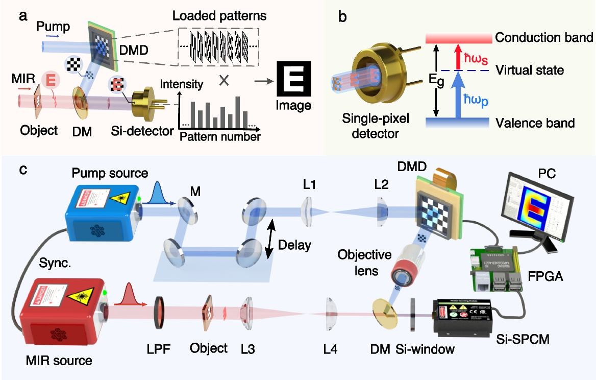
The research team led by Prof. Heping Zeng and Prof. Kun Huang in East China Normal University (ECNU) have introduced ND-2PA into a single-pixel computational imaging framework, creating an integrated encoding–detection system (Fig. 1). In this scheme, spatially structured NIR pump light acts as an all-optical mask for the MIR signal. When the pump and signal photons jointly interact within a silicon detector, their energies exceed the bandgap, producing a measurable photocurrent (Fig. 2). Each structured pump pattern leaves a distinct “projection” in the detector response, which is later used for computational reconstruction.
By leveraging mature NIR modulation techniques, the system bypasses the diffraction limits of long-wavelength modulation and achieves ~7 μm spatial encoding precision, corresponding to 11 μm imaging resolution. These results experimentally confirm the feasibility and performance advantages of the approach.

Figure 2: Experimental setup of mid-infrared two-photon computational imaging
Chemical Selectivity and Applications
Beyond principle validation, the team demonstrated the potential of this approach for multispectral and chemical-selective imaging. In experiments with thin films of polystyrene (PS) and polyvinyl chloride (PVC), the system successfully distinguished different absorption fingerprints across the 2.5–3.8 μm band (Fig. 3), underscoring its promise for chemical recognition and molecular sensing.

Figure 3: Mid-infrared selective imaging of chemical thin-film samples
Looking forward, the technique could be combined with high-numerical-aperture optics and large-area detectors to achieve megapixel-level resolution for high-definition imaging. Optimizing pump wavelengths and detector materials may further extend the operational band, enhancing molecular fingerprint identification. Meanwhile, the synchronous pulsed gating could provide depth resolution, paving the way for high-resolution MIR 3D imaging.
For more details, please read our recent publication: Huijie Ma, Kun Huang*, Jianan Fang, Ziyu He, Yan Liang, and Heping Zeng*, “Mid-infrared single-pixel imaging via two-photon optical encoding”, Photonix 6, 34 (2025).
Kun Huang received his Ph.D. degree from École Normale Supérieure (ENS-Paris) in 2015, followed by postdoctoral research at Université Pierre et Marie Curie (UPMC), France. He is currently a Professor at East China Normal University (ECNU). His research focuses on single-photon detection, computational imaging, nonlinear frequency upconversion, and mid-infrared spectroscopy. He has co-authored more than 100 peer-reviewed papers in leading journals such as Nature Photonics, Nature Communications, and Science Advances. He also serves on the editorial boards of European Physical Journal D, Ultrafast Science, PhotoniX, and Infrared and Laser Engineering.
Follow the Topic
-
PhotoniX
PhotoniX aims to present brave endeavors in promoting X-disciplinary research, latest progress of engineering applications and breakthroughs in scientific discoveries, all enabled by photonics. Original scientific letters, articles, reviews, and technology progress reports are equally welcome.

Related Collections
With Collections, you can get published faster and increase your visibility.
Photonics X Metaverse
Metaverse is a comprehensive concept because it is not a single technology, but an expansive, interconnected framework composed of multiple disciplines. Therefore, to fully realize the metaverse, it is necessary to integrate expertise from traditionally siloed fields. Photonics, among them, is acting as a powerful catalyst, driving waves of innovation across all layers of the metaverse hardware ecosystem. This special Issue aims to highlight the latest breakthroughs and insights at the intersection of metaverse and photonics and to foster continuous, cross-disciplinary dialogue and collaboration.
Scope:
Topic 1: Photonics-powered near-eye displays (magnifiers, birdbaths, waveguides, etc.)
Topic 2: Photonics-powered microdisplays (Micro LED, Micro OLED, LCoS, DMD, laser, etc.)
Topic 3: Photonics-powered three-dimensional displays (holography, light field, etc.)
Topic 4: Nanophotonics-powered lenses (freeform lenses, Fresnel lenses, pancake lenses, metalenses, contact lenses, etc.)
Topic 5: Biophotonics-powered bionics (bionic eyes, retinal implants, etc.)
Publishing Model: Open Access
Deadline: Dec 31, 2026
Solar Light-Matter Interactions: Energy Regulation, Conversion and Its Interdisciplinary Applications
Scope:
Topic 1: Fundamental physical and chemical mechanisms underlying solar light-matter interactions
Topic 2: Design, fabrication, and solar radiation regulation performance of micro/nanostructures (e.g., metamaterials, plasmonic materials, porous materials)
Topic 3: High-efficiency solar photothermal/photovoltaic conversion devices and systems
Topic 4: Daytime radiative cooling materials, devices, and their engineering applications
Topic 5: Applications of solar energy conversion technologies in water treatment, environmental remediation, building energy efficiency, and other related fields
Topic 6: Research on the photothermal dynamic regulation mechanisms between solar light and organisms (including humans and other mammals, etc.)
Publishing Model: Open Access
Deadline: Ongoing


Please sign in or register for FREE
If you are a registered user on Research Communities by Springer Nature, please sign in