
With the development of electronic and information technology, electronic devices are expected to be more miniaturized, multifunctional and intelligent. In the future, by integrating electronic devices into multifunctional micro/nano-systems and large-scale networks for environmental monitoring, human-machine interfacing, biomedical diagnosis/therapy and so on, everything could be connected to the Internet for information interaction and intelligent identification. Thus, the use of a huge number of electronic devices needs to solve the problem of limited battery life to achieve self-powered. On the other hand, it is necessary to establish the direct interaction mechanism between electronics and external environment to realize the active information acquisition.
In 2012, triboelectric nanogenerator (TENG) as an emerging energy technology was invented by Wang’s group, which is derived from Maxwell’s displacement current. The TENG has been exhibited for harvesting human kinetic and ambient mechanical energy, which can act as a power supply and self-powered sensors for personal electronics, environmental monitoring, health devices, and so on. In recent years, by coupling the triboelectricity and semiconductor properties, tribotronics, as a novel research field has been proposed, which has demonstrated various triboelectrification-controlled electronics and established direct modulation mechanism by external mechanical stimuli. However, the interactive interfaces between external environment and electronics in current tribotronic devices are all in the macro scale, which has limited the integration and modularization of tribotronics. When the size scales down to the micro/nano-range, whether the modulation effect still exists is a critical question for tribotronics.
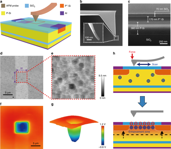
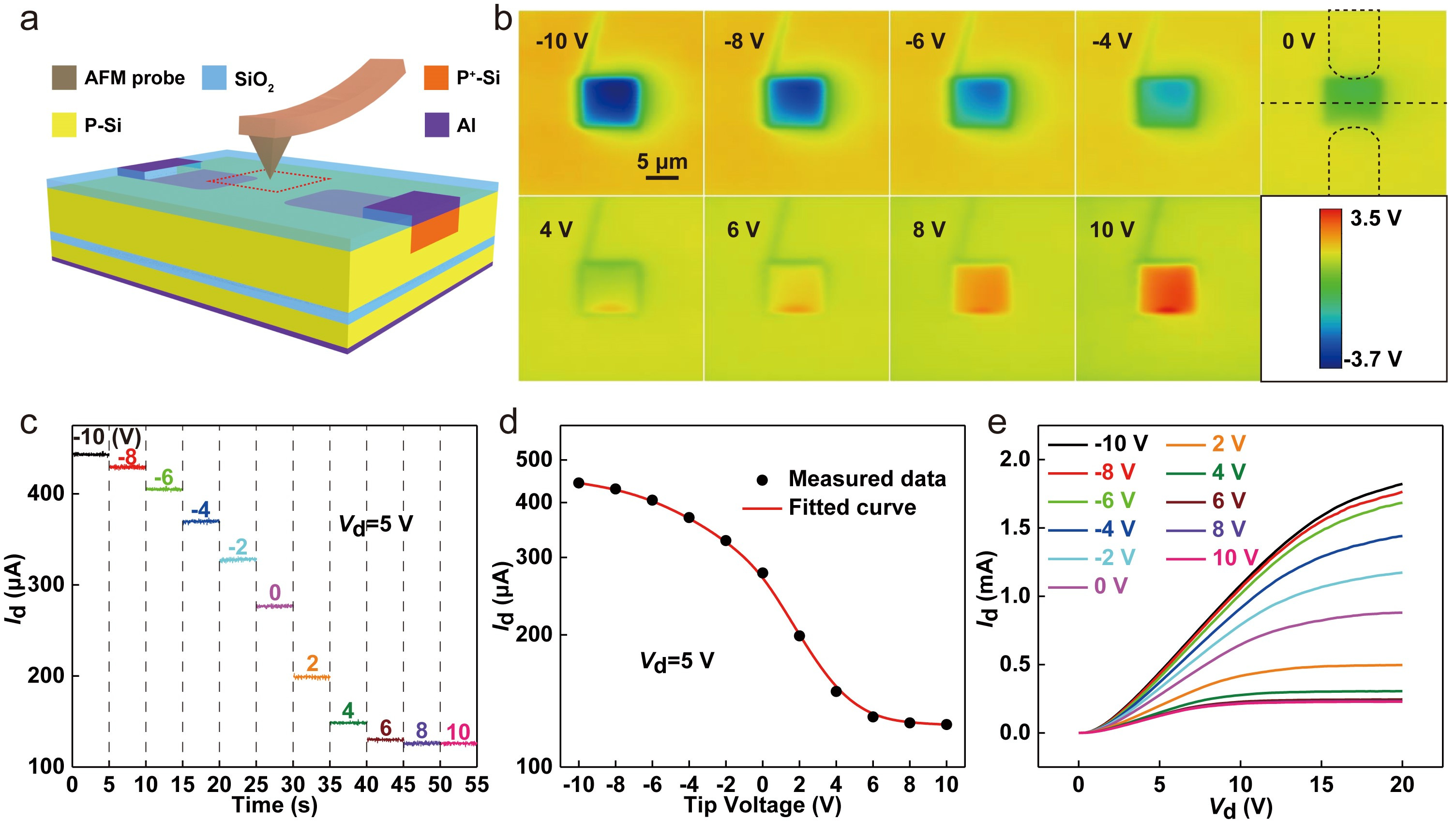
To address this problem, we studied the nanoscale triboelectrification-gated transistor (NTT), by the coupling of contact-mode atomic force microscopy (C-AFM) and scanning Kevin probe microscopy (SKPM). In the NTT, nanoscale triboelectrification is generated by using an AFM tip with a diameter of 20 nm to scan the dielectric layer above the channel region (5 μm×5 μm), which can further tune the drain current of the NTT. The potential difference induced by nanoscale triboelectrification is enhanced and reaches a saturation value of -1.5 V with the increasing of scan number and contact force and the decreasing of scan speed, respectively. The corresponding drain current increases from 138 μA to 280 μA. The modulation effect has also been demonstrated when scan area is changed and charge dissipation exists. Moreover, the potential difference various from -5 V to 2 V by an applied tip voltage, which can serve as a rewritable floating gate to tune the drain current from 125 μA to 443 μA. This work has realized the nanoscale triboelectric modulation on electronics, which could provide a deep understanding for the theoretical mechanism of tribotronics and may have great applications in nanoscale transistor, micro/ nano-electronic circuit and nano-electromechanical system.
For more information, please refer to our recent publication in Nature Communications: Nanoscale Triboelectrification Gated Transistor (https://doi.org/10.1038/s41467-020-14909-6).
Follow the Topic
-
Nature Communications

An open access, multidisciplinary journal dedicated to publishing high-quality research in all areas of the biological, health, physical, chemical and Earth sciences.
Related Collections
With Collections, you can get published faster and increase your visibility.
Women's Health
Publishing Model: Hybrid
Deadline: Ongoing
Biosensing
Publishing Model: Hybrid
Deadline: Jun 30, 2026

Please sign in or register for FREE
If you are a registered user on Research Communities by Springer Nature, please sign in