Optical and Radiofrequency Transparent Metadevices
Published in Electrical & Electronic Engineering
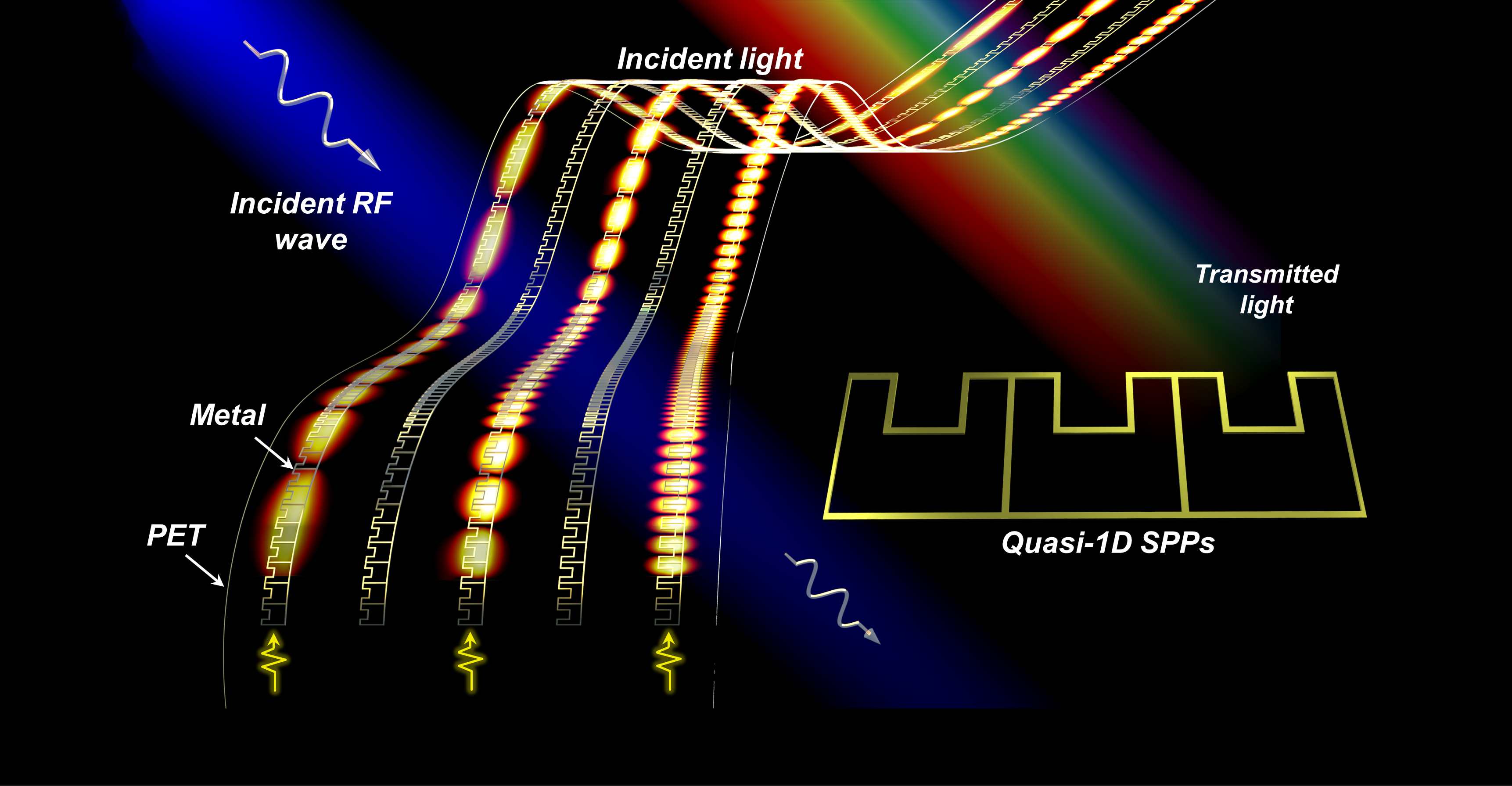
Quasi-one-dimensional surface plasmon polariton structures
For a long time, most of the research on transparent electronics has been devoted to optical transparent conductor materials, and it can even be said to rely on materials science. Even that, these devices have low optical transmittance, low operating efficiency and an inability to achieve radiofrequency (RF) transparency. Here, we presents the quasi-one-dimensional (quasi-1D) surface plasmon polaritons (SPPs) structures, utilizing structured metals to realize optical and RF transparent electronics, regardless of whether the conductor material is transparent or not, let alone the preparation of expensive transparent conductor materials.
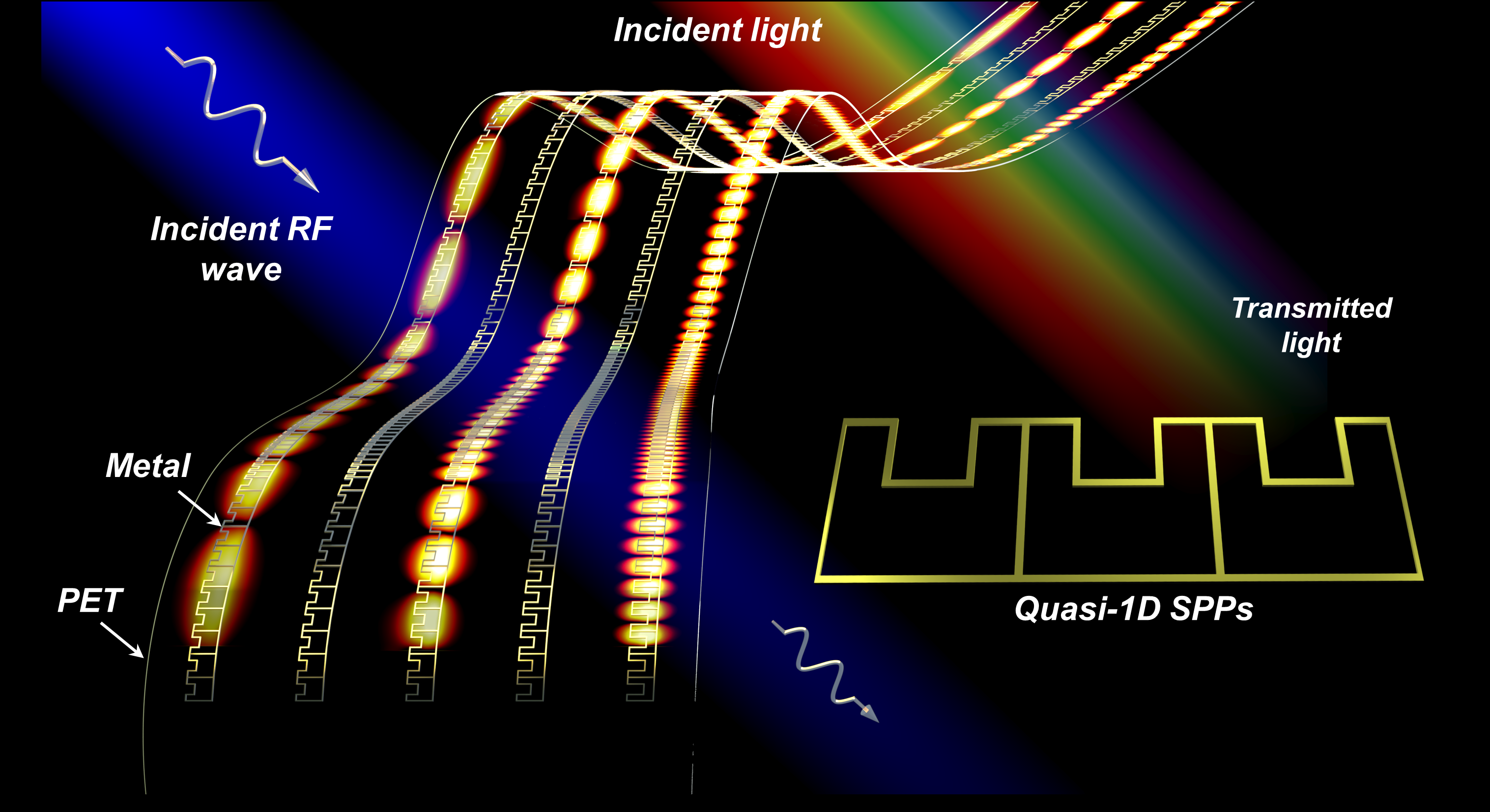
Our quasi-1D SPPs structures are composed of subwavelength unit cells created from fine metallic lines printed on a polyethylene terephthalate (PET) substrate (Fig. 1). The electromagnetic energy in SPPs mode can be effectively confined and channelled by the metallic lines, whilst offering excellent transmittances for both optical and RF incidences.
Optical and RF transparent metadevices
To intuitively show the great potential and feasibility of the proposed quasi-1D structured SPPs for developing transparent SPPs metadevices, we demonstrate the shaped SPPs waveguides with great topological robustness and the converter from SPPs wave to space wave, which indicate the special superiorities in transmission and radiation metadevices, respectively.
Since the quasi-1D structured SPPs own high confinement, the energy can be concentrated and channeled along the proposed structures, showing excellent topological robustness for realizing arbitrary-shape SPPs waveguides. Figure 2a illustrates the photographs of the “SPP” shaped quasi-1D SPPs waveguides, which exhibit excellent transparency and are nearly invisible. The shape of the letters “SPP” is formed by arranging the quasi-1D structured SPPs unit cells. As depicted in Fig. 2 b and c, the characters of “SPP” are portrayed with highly enhanced and confined electric fields.
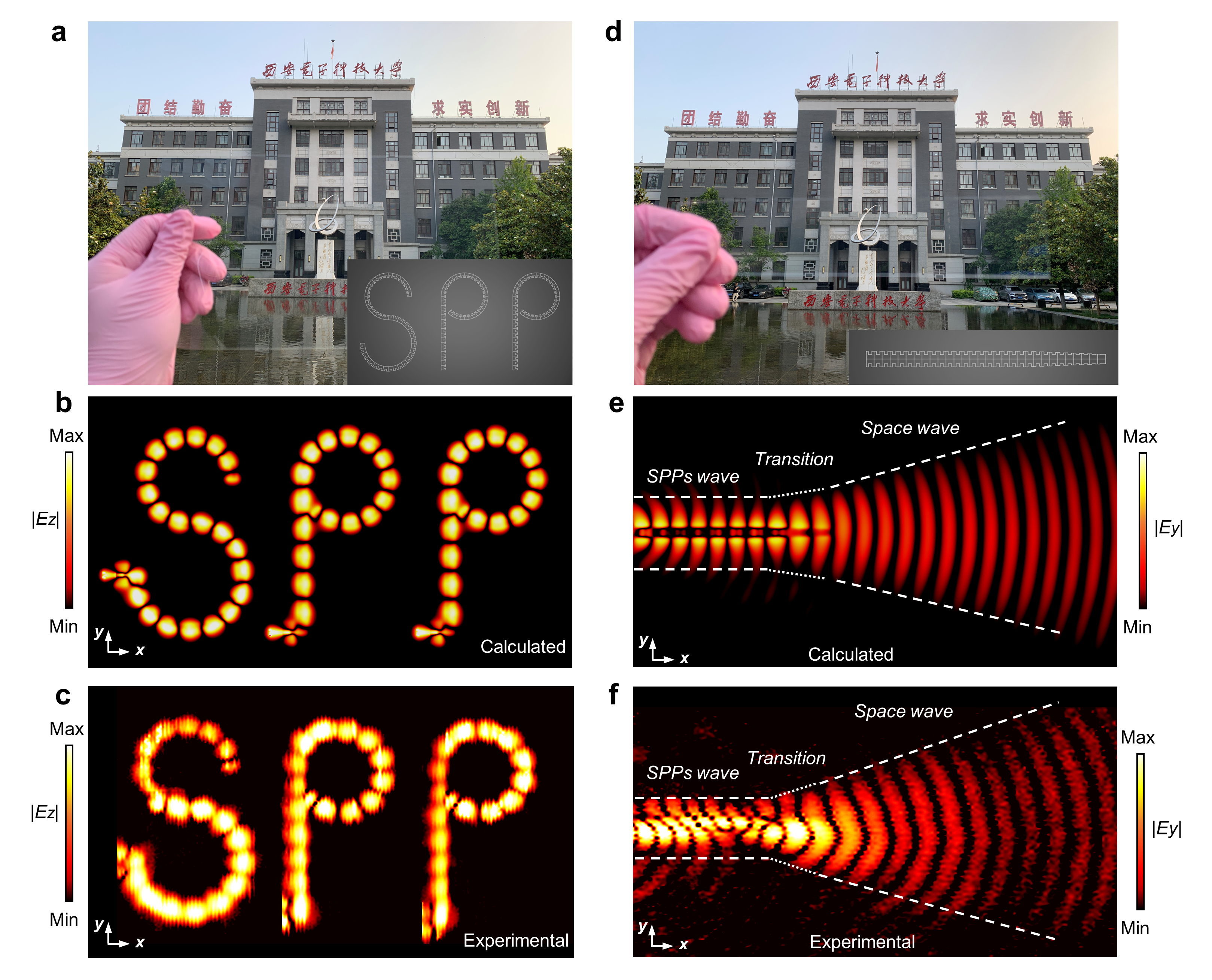
Further, the energy confinement can be manipulated by adjusting the geometrical parameters. Hence, we fabricated the converter from SPPs wave to space wave. By gradually reducing the groove depth of the quasi-1D structures, the energy confinement of the structures is gradually weakened, and the matching from the strongly confined SPPs waves to the weakly confined space waves is finally completed. Figure 2d illustrates the photographs of the quasi-1D structured converter from SPPs wave to space wave, and the configuration is nearly invisible. Figure 2 e and f exhibit the calculated and experimental electric field distributions of the converter. It is observed that the groove depth in the first half of the converter is constant to support strongly confined SPPs waves, and the groove depth in the second half decreases linearly to 0. In this way, confinement of the SPPs mode gradually decreases, and finally the SPP waves are transformed completely into space wave to form stable endfire radiation.
These results reveal the great potential of the proposed quasi-1D structured SPPs in generating a series of optical and RF transparent metadevices, such as conformal waveguides, antennas, sensors, etc.
Optical and RF transparent wireless communication scheme
In nowadays complex electromagnetic environment where various electronic devices coexist, the demand for integrated communication, optical stealth, and electromagnetic stealth is becoming more and more intense. Many scenarios (e.g., solar energy harvesting, urban densification communication, and vehicle-mounted communication) urgently seek for a wireless communication system that can provide high signal strength, excellent optical and RF transmittance. Such a communication system can easily be integrated into various transparent objects (e.g., windows of office buildings, vehicle-mounted glass, digital screens, solar panels) without deteriorating the communication and energy collection of the original electronic devices. The proposed optical and RF transparent metadevices make this long-standing vision a reality.
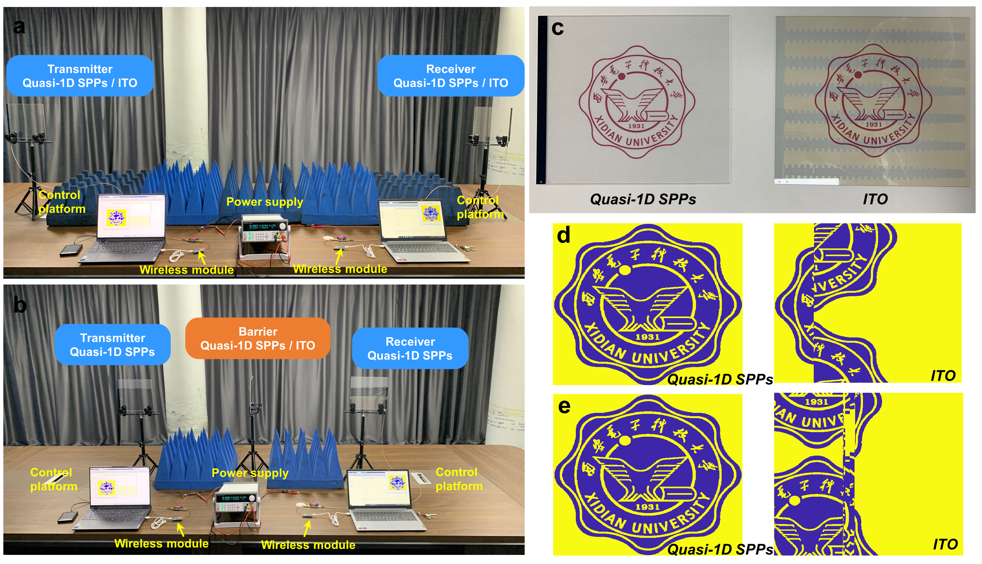
Figure 3 | Experimental validation of the optical and RF transparent metadevices based wireless communication scheme. a Quasi-1D SPPs based/ITO based data transfer under the same transmitted power of -40 dBm, without barrier. b Quasi-1D SPPs based data transfer under the transmitted power of -48 dBm, with the quasi-1D SPPs/ITO barrier. c Comparison photographs of the quasi-1D SPPs transceiver and the ITO transceiver. d Comparison of image quality between quasi-1D SPPs based/ITO based data transfer without the barrier. e Comparison of image quality between quasi-1D SPPs/ITO barrier in quasi-1D SPPs based data transfer.
Figure 3 illustrates the experimental validation of the optical and RF transparent metadevices based wireless communication scheme. Detailedly, Fig. 3a shows the quasi-1D SPPs based/traditional indium tin oxide (ITO) based data transfer system without barrier. Figure 3b demonstrates the quasi-1D SPPs based data transfer system with quasi-1D SPPs/ITO barrier. The distance between the transmitter and the receiver is set as 1 m to better shield the radiation wave and strictly evaluate the impact of RF transmittance on data transmission. Correspondingly, the transmitting power is adjusted to satisfy Friis’ transmission formula, and the quasi-1D SPPs transceiver and ITO transceiver are adopted as the barrier for comparison.
Figure 3c exhibits the comparison photographs of the fabricated quasi-1D SPPs transceiver and ITO transceiver, and the square resistance of ITO is 1 Ω/square, which is a common value in high-conductivity devices. Obviously, the quasi-1D SPPs transceiver has higher optical transmittance, and this method not only brings the optical transmittance improvement, but also presents an invisible configuration. Figure 3d depicts the comparison of image quality between the quasi-1D SPPs based and the ITO based data transfer systems without the barrier. Since the traditional method relying on ITO is subject to the materials’ intrinsic properties: conductivity (carrier density) and optical transparency are mutually restricted, even if the ITO with high conductivity (1 Ω/square) is adopted, the operation efficiency in wireless communication systems will deteriorate extremely , which leads to a sharp drop in signal strength and communication distance, and the image received by the ITO system is severely distorted. Figure 3e demonstrates the comparison of image quality between quasi-1D SPPs/ITO barriers. ITO is unable to possess RF transparency, hence ITO-based devices will block the communication of other devices, which is not conducive to the integration of communication systems. Therefore, using the quasi-1D SPPs transceiver in the communication path can obtain excellent communication quality, while adopting the ITO devices will greatly deteriorate the data transmission and against the integrated communication.
This research will help further improve the performance of next-generation transparent communication devices.
Follow the Topic
-
Nature Electronics
This journal publishes both fundamental and applied research across all areas of electronics, from the study of novel phenomena and devices, to the design, construction and wider application of electronic circuits.




Please sign in or register for FREE
If you are a registered user on Research Communities by Springer Nature, please sign in