Performance limits of hexagonal boron nitride as an insulator for scaled CMOS devices
Published in Electrical & Electronic Engineering

In 2016, when I had just started to work on my PhD thesis, my supervisor, Prof. Tibor Grasser, approached me with an apparently small research question: “How can it be that hBN is considered such a promising insulator [1] if its valence band edge is so close to the valence band of most 2D semiconductors [2] and its permittivity of about 4 is so small [3]? Could you quickly calculate the tunneling currents in scaled structures, they should be going through the roof?” Fully motivated by an interesting research question, I set out to answer it. We decided to use a simple semi-classical description of the tunneling current. After having acquired some familiarity with the tools, most disconcertingly, I could not reproduce experimental results taken from literature. It was unclear at that point whether this discrepancy resulted from the possibly too simplistic tunneling model, which might not be applicable to layered 2D structures, or defects and impurities in the measured hBN samples which we did not account for.
After having kept the topic on the back-burner, our interest was rekindled when we obtained new transistors from one of our collaborators, the group of Prof. Thomas Mueller. They had fabricated transistors with exfoliated hBN as a gate insulator [4]; using the hBN from Dr. Takashi Taniguchi at the National Institute of Materials Science (Japan), which has been shown by multiple groups world-wide to be of exceptional quality [5]. I extensively characterized the transistors and quickly realized that all devices suffered from excessive leakage currents across the h-BN. When comparing our results with leakage currents reported in literature we realized that others faced the same problems. Scientists from all over the world used hBN obtained with different synthesis methods and qualities and all reported high leakage currents [6,7], that is to say if they reported leakage currents and used hBN on its own rather than in combination with other insulators. This realization confirmed our initial hypothesis but did not ease our doubts, as despite the substantial research efforts targeted at hBN, the reported data on leakage currents was scarce. In particular, it was unclear if these large tunneling currents were a consequence of the fundamental material properties of hBN or indicated some quality issues which would eventually be resolved.
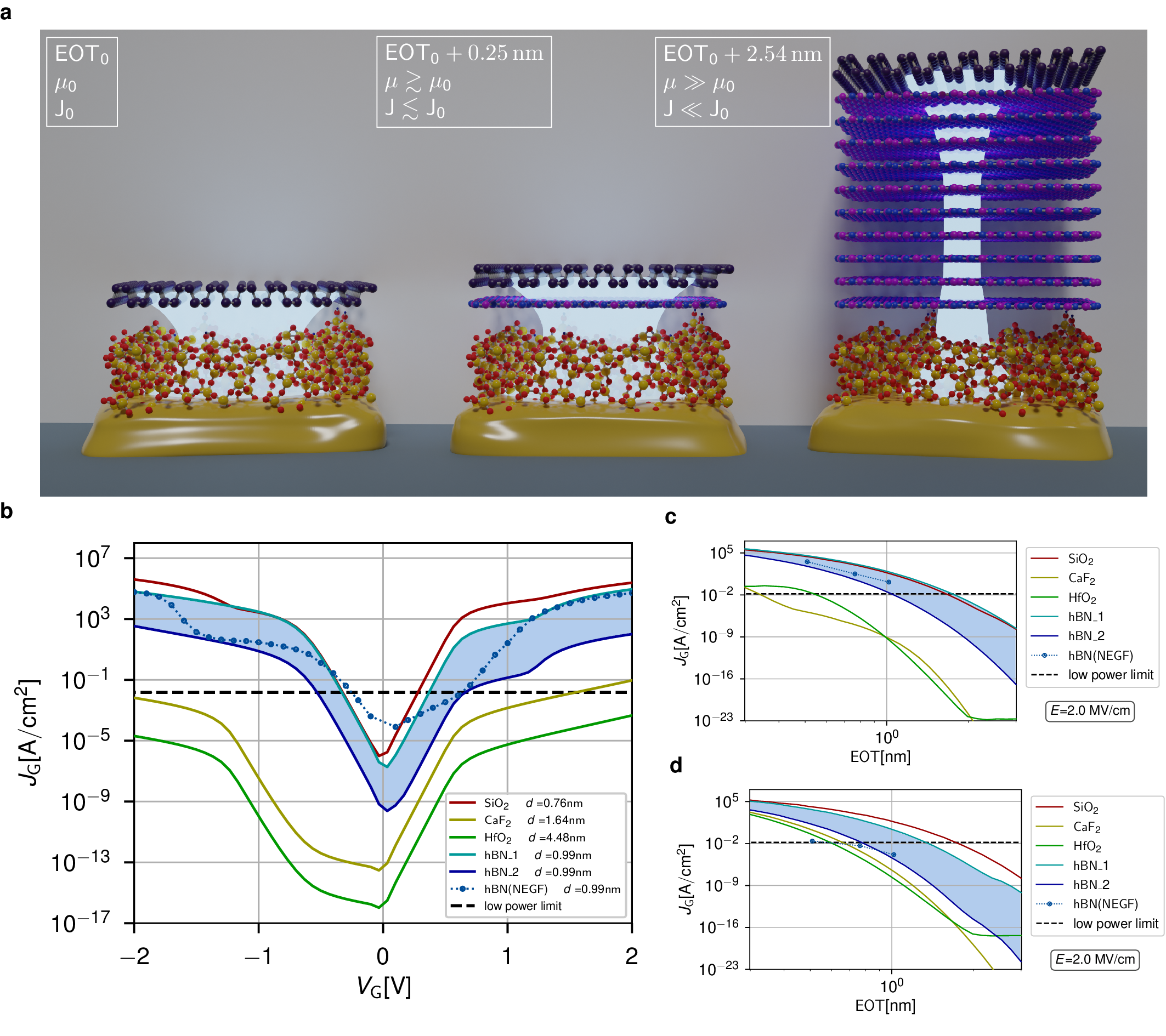
The lack of experimental data compelled us to revisit our initial theoretical work. If we confirmed the validity of our theoretical predictions, this would show that all efforts undertaken to develop 2D material based transistors based on hBN as a gate insulator would suffer from a serious limitation: the thickness of hBN could not be scaled down to the required level due to excessive leakage currents, see Figure 1a. However, many people in the community we discussed this issue with seemed to be unaware of this potential problem and its implications. Many attributed the high leakage currents to defects in the hBN and to some issues with the synthesis of hBN which is still in its early stages and would improve over time as the technology matured. Our simulation data however described ideal, defect-free hBN and indicated that the intrinsic material properties were the root cause for the high leakage currents which would as such not improve beyond a certain point by optimized processing.
In order to validate our calculations, we reached out to Prof. Mikhail I. Vexler with whom we had extensive discussions and performed multiple cross-checks to confirm our results. The most serious remaining doubt was thus related to the validity of our semi-classical approach applied to a layered material. After discussing this problem with Prof. Mathieu Luisier, an expert in ab initio carrier transport modeling, we decided to perform fully quantum mechanical ab initio calculations of charge transport through hBN. It was reassuring to find from this entirely different perspective that the calculated ab initio currents were well within the range which we had obtained with the semi-classical approach, see Figures 1b-d. This success gave us the confidence needed to finally tell the story we had been working on for nearly four years by then: While hexagonal boron nitride is a fascinating material with many promising applications in nano- and optoelectronics (such as resistive switching memories [8] and neuromorphic circuits [9]), the excessive leakage currents through hBN render it unsuitable as a gate insulator for scaled CMOS logic. This observation makes it clear that there is currently a lack of gate insulators which are compatible with 2D materials and at the same time sufficiently block currents to allow for continued scaling [10]. Thus, towards the end of our Perspective article [11] we review the current blocking potential of several other insulators. We think that our findings represent an important contribution to the advancement of 2D materials based nanoelectronics and as such will help to develop novel technologies which will be useful for our society.

For more information please check out our article “The performance limits of hexagonal boron nitride as an insulator for scaled CMOS devices based on two-dimensional materials” published in Nature Electronics [11].
References:
[1] Zhang, K. et al. Two dimensional hexagonal boron nitride (2D-hBN): Synthesis, properties and applications. Journal of Materials Chemistry C, 5(46), 11992–12022, (2017).
[2] Strand, J., Larcher, L., & Shluger, A. L. Properties of intrinsic point defects and dimers in hexagonal boron nitride. Journal of Physics: Condensed Matter, 32, 055706, (2020).
[3] Laturia, A., Van de Put, M. L., & Vandenberghe, W. G. Dielectric properties of hexagonal boron nitride and transition metal dichalcogenides: from monolayer to bulk. Npj 2D Materials and Applications, 2(1), 6, (2018).
[4] Paur, M. et al. Electroluminescence from multi-particle exciton complexes in transition metal dichalcogenide semiconductors. Nature Communications, 10(1), 1–7, (2019).
[5] Zastrow, M. Meet the crystal growers who sparked a revolution in graphene electronics. Nature, 429–432, (2019).
[6] Britnell, L. et al. Electron tunneling through ultrathin boron nitride crystalline barriers. Nano Letters, 12(3), 1707–1710, (2012).
[7] Jang, S.K. et al. Synthesis and Characterization of Hexagonal Boron Nitride as a Gate Dielectric. Scientific Reports, 6(2003), 30449, (2016).
[8] Puglisi, F. M. et al. 2D h -BN based RRAM devices. IEDM Tech. Dig., 874–877, (2016).
[9] Chen, S. et al. Wafer-scale integration of two-dimensional materials in high-density memristive crossbar arrays for artificial neural networks. Nature Electronics, 3(10), (2020).
[10] Illarionov, Yu.Yu. et al. Insulators for 2D nanoelectronics: the gap to bridge. Nature Communications, 11(1), (2020).
[11] Knobloch, T. et al. The performance limits of hexagonal boron nitride as an insulator for scaled CMOS devices based on two-dimensional materials. Nature Electronics, 2, (2021).
Copyrights of the poster image: Jean Favre, Visualization Scientist at CSCS.
Follow the Topic
-
Nature Electronics
This journal publishes both fundamental and applied research across all areas of electronics, from the study of novel phenomena and devices, to the design, construction and wider application of electronic circuits.


Please sign in or register for FREE
If you are a registered user on Research Communities by Springer Nature, please sign in
Congratulations, outstanding work in the field of 2D materials !