Surface/Interface Engineering for High‑Resolution Micro‑/Nano‑Photodetectors

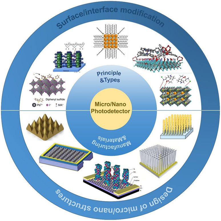
As artificial intelligence and miniaturized electronics surge forward, conventional photodetectors struggle to deliver the resolution, speed and energy efficiency required for next-generation imaging, sensing and human–machine interaction. Now, a team led by Professor Wei Chen at Tsinghua University has published a comprehensive roadmap on surface/interface engineering that turns micro-/nano-scale photodetectors into ultra-sharp “electronic eyes”. The work appeared in Nano-Micro Letters.
Why Surface/Interface Engineering Matters
• Defect Healing: Atomic-level passivation and functional-group grafting suppress interfacial traps, slashing dark current and boosting signal-to-noise ratio.
• Band-gap Sculpting: van-der-Waals heterojunctions, quantum wells and strain gradients tailor the spectral window from deep-UV to long-wave infrared without extra filters.
• Light-management: Elliptical gratings, pyramidal textures and plasmonic nano-cavities extend the optical path, enabling >90 % absorption in films thinner than 50 nm.
• Mechanical Bridging: Hydrophobic–hydrophilic patterning and buffer layers reconcile soft organics with rigid inorganics, giving flexible devices a bending radius <1 mm while maintaining pixel pitch down to 1 µm.
Innovative Design and Features
• Material Menu: 2D black phosphorus with strain-tunable bandgap, perovskite nanowire arrays for full-colour imaging, TMDC/graphene heterostacks for picosecond response, and lead-free CsSnBrx inks for green manufacturing.
• Processing Toolkit: ALD-grown 1-nm Al2O3 passivation shells, EHD printing of 1 µm pixels, plasma-enhanced CVD for wafer-scale TMDCs, and self-assembled monolayers that lower interfacial traps by an order of magnitude.
• Architecture Gallery: 1D nanonail forests, 2D lateral p–n heterojunctions, 3D pyramid-on-pyramid textures, and resonant cavities that fold a 1550 nm beam into a 300 nm active layer.
Applications and Future Outlook
• Thermal Imaging: Passivated InGaAs/AlGaN pixel arrays resolve 20 mK temperature differences at 1 kHz frame rates for night-vision and medical diagnostics.
• Flexible Wearables: Transfer-printed single-crystal perovskite sheets wrapped around a robotic finger provide 317 ppi imaging during grasping tasks.
• Bio-inspired Vision: A hemispherical 1 µm-pitch nanowire retina coupled to liquid-metal nerves mimics human-eye resolution and is implantable for vision restoration.
• Catalytic Sensing: TiO2/BaTiO3 core–shell nanorods double photoelectrochemical water-splitting efficiency while acting as self-powered UV monitors.
Challenges and Opportunities
The review pinpoints reproducibility of sub-10 nm interfaces, long-term stability under moist bio-environments, and CMOS-compatible pitch scaling below 200 nm as the next grand challenges. Future research will marry machine-learning-guided multi-parameter optimization with roll-to-roll nano-imprint lithography to deliver wafer-scale, defect-free electronic eyes for intelligent systems.
This comprehensive roadmap offers device engineers, materials scientists and circuit designers a unified vocabulary for transforming any photodetector—old or new—into a high-resolution, low-power, spectrum-agile imaging engine.
Editor of Nano-Micro Letters, which is an Open-Access, peer-reviewed journal reported papers that have at least one dimension ranging from a few sub-nanometers to a few hundreds of micrometers. The journal is published by Springer Nature and indexed by SCI, EI, SCOPUS, Pubmed, etc. The 2025 JCR Impact Factor is 38.5. The 2025 CiteScore is 58.9.
Follow the Topic
-
Nano-Micro Letters
Nano-Micro Letters is a peer-reviewed, international, interdisciplinary and open-access journal that focus on science, experiments, engineering, technologies and applications of nano- or microscale structure and system in physics, chemistry, biology, material science, and pharmacy.


Please sign in or register for FREE
If you are a registered user on Research Communities by Springer Nature, please sign in