There’s Not Enough Room at the Bottom
Published in Electrical & Electronic Engineering, Materials, and Physics

Background
In the past decades, Si FETs shrank their lateral sizes continuously, following the famed Moore’s law [1]. The footprint of a single transistor has been scaled from a few tens of micron-meter in the early days, down to sub-10 nm (such as the recent development often referred to as the ‘3 nm node’, although the definition varies from different foundries) now. Apparently, further decreasing the linewidth of transistors will soon approach the physical limit: a single atom. And it seems to be high time we said goodbye to the Moore’s law, as there’s not enough room at the bottom to pack more FETs within the unit area of a Si chip surface. – Unless one can find another way out, for example, going upwards such as the 2.5D/3D IC with chiplets.
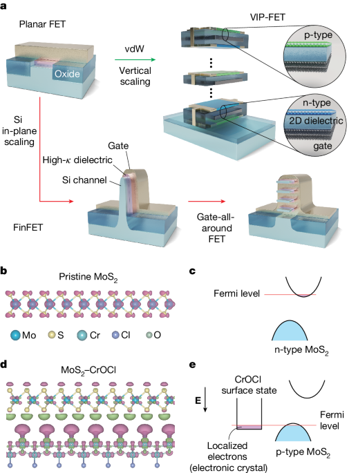
On the contrary to conventional semiconductors, the van der Waals ones demonstrate a strong capability of z-dimensional stacking, theoretically allowing for an unlimited number of layers. This is considered one of the most fascinating aspects of vdW nanoelectronics, and indeed has become a pursuit attracting much attention [2-5], especially when recent progresses have been made in large scale production of high quality 2D semiconducting crystals [7-10] as well as the Ohmic contact approaching the quantum limit [11-12]. However, being studied for over two decades, 2D semiconductors are still at a status of ‘being at the verge of, but not yet quite there’ for a successful 3D vertical integration. The main challenge remains in the lack of a controllable and stable doping method that can easily switch the polarity of a van der Waals (vdW) semiconducting FET from n-type (which is the conventional type for most transition metal dichalcogenides, such as TMDs) to p-type.
Experimental results
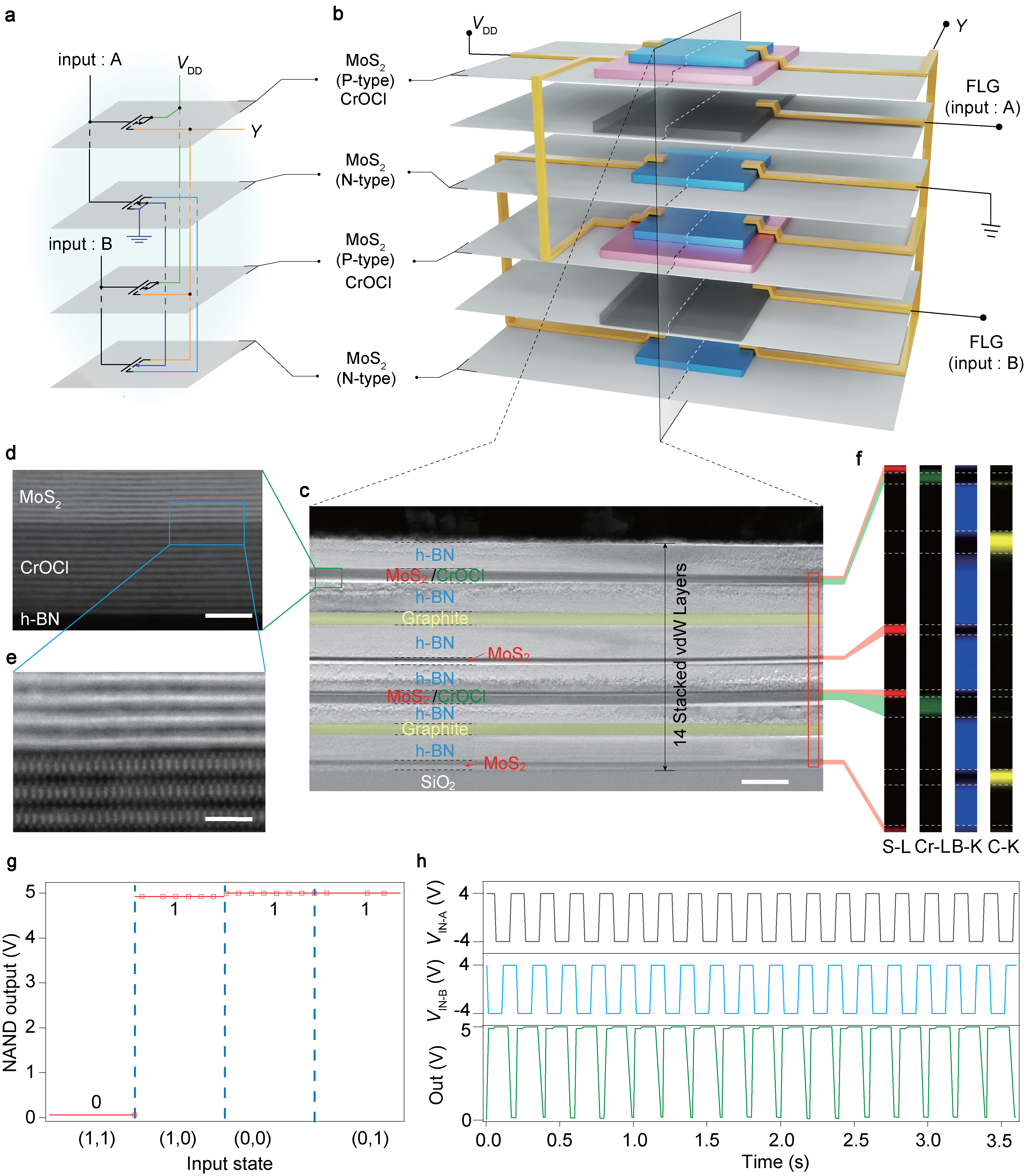
We brought few-layered TMDs into contact with a few-layered antiferromagnetic insulator CrOCl. Surprisingly, we found that, unlike the usually manifested n-type nature, few-layered TMDs (including MoS2, WSe2, and MoSe2) interfaced with few-layered CrOCl systematically turn into p-type and display high ON-state current, low hysteresis, large ON-OFF ratio, as well as excellent air stability. The major findings of our work are summarized in the following:
- We have demonstrated an elaborated doping method that can readily shift the polarity of a 2D semiconducting field-effect transistor (FET) from n-type to p-type by utilizing vdW interfacial coupling, which turned out to be rather universal (MoS2, WSe2, and MoSe2 have been tested).
- Our density functional theory (DFT) calculations suggest that this interfacial coupling induced polarity inverse is likely a result of quantum effect of the charge transfer from TMDs to CrOCl and followed by electronic crystal formation, which is a universal effect at the interface between TMDs and other layered insulators with high work function (WF) in the valence band.
- Based on this method, we have successfully stacked complementary 2D FETs up high into the z-dimension (maximum 14 vdW layers here in our work, shown in Fig. 1) -- a degree of freedom that the Si tech industry has been looking after but could never reach so far.
This breakthrough opens up a new door towards the free-design of 3D-interconnected integrated circuits using vdW semiconductors as building blocks, which represents a distinct departure from the current route of 2D in-plane scaling of Si complementary MOSFETs.
For more details, please see the original version of the manuscript in Nature
https://www.nature.com/articles/s41586-024-07438-5
References
[1] Cao, W. et al. The future transistors. Nature. 620, 501-515 (2023).
[2] Kim, K. S. et al. Seamless monolithic three-dimensional integration of single-crystalline films by growth. Preprint at https://doi.org/10.48550/arXiv.2312.03206 (2023).
[3] Tong, L. et al. Heterogeneous complementary field-effect transistors based on silicon and molybdenum disulfide. Nat. Electron. 6, 37–44 (2023).
[4] Ran, Y. et al. Large-scale vertically interconnected complementary field-effect transistors based on thermal evaporation. Small https://doi.org/10.1002/smll.202309953 (2023).
[5] Jayachandran, D. et al. Three-dimensional integration of two-dimensional field-effect transistors. Nature 625, 276–281 (2024).
[6] Lu, D. et al. Monolithic three-dimensional tier-by-tier integration via van der Waals lamination. Nature https://doi.org/10.1038/s41586-024-07406-z (2024).
[7] Xu, X. et al. Seeded 2D epitaxy of large-area single-crystal films of the van der Waals semiconductor 2H MoTe2. Science 372, 195 (2021).
[8] Wang, Q. et al. Layer-by-layer epitaxy of multi-layer MoS2 wafers. National Science Review 9: nwac077 (2022).
[9] Kwon, J. et al. 200-mm-wafer-scale integration of polycrystalline molybdenum disulfide transistors. Nature Electronics https://doi.org/10.1038/s41928-024-01158-4 (2024).
[10] Liu, A. et al. Selenium alloyed tellurium oxide for amorphous p-channel transistors. Nature https://doi.org/10.1038/s41586-024-07360-w (2024).
[11] Shen, P.-C. et al. Ultralow contact resistance between semimetal and monolayer semiconductors. Nature 593, 211–217 (2021).
[12] Li, W. et al. Approaching the quantum limit in two-dimensional semiconductor contacts. Nature 613, 274–279 (2023).
Follow the Topic
-
Nature
A weekly international journal publishing the finest peer-reviewed research in all fields of science and technology on the basis of its originality, importance, interdisciplinary interest, timeliness, accessibility, elegance and surprising conclusions.

Related Collections
With Collections, you can get published faster and increase your visibility.
Carbon Dioxide Removal
Publishing Model: Hybrid
Deadline: Jan 16, 2027


Please sign in or register for FREE
If you are a registered user on Research Communities by Springer Nature, please sign in