Toward three-dimensional hybrid inorganic/organic optoelectronics based on GaN/oCVD-PEDOT structures
Published in Electrical & Electronic Engineering

Light emitting diodes (LEDs) based on the inorganic semiconductor gallium nitride (GaN) replaced the classical incandescent ("Edison") light bulb and truly enabled a new era in lighting that was honored by the Noble Prize in Physics 2014. Although the epitaxial growth of p-type GaN was an essential part of this innovation that became state-of-the-art in two-dimensional (2D) LED manufacturing today, it has rather poor current spreading properties to enable next-generation LEDs based on three-dimensional (3D) core-shell architecture.
To overcome this obstacle, we decided to find a proper substitute for the inorganic p-type GaN and looked into the materials typically employed in organic light emitting diodes (OLEDs). Although OLEDs have not been honored with the Noble Prize, they employ a very extraordinary class of materials that was worth the Nobel Prize in Chemistry 2000 – the "Conductive Polymers". These materials have a conjugated carbon backbone that forms a delocalized π-electron system and enables efficient charge transport within the polymer chain. Poly(3,4-ethylenedioxythiophene) mixed with poly(styrenesulfonate), better known as "PEDOT:PSS", is an attractive organic p-conductor. The hydrophilic PSS is required because it enables liquid deposition on simple, planar substrates used by the OLED industry.
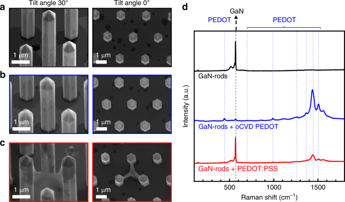
However, it is indeed very challenging to obtain conformal, pinhole-free coatings of PEDOT:PSS on complex, 3D substrates such as microrods or nanowires. To overcome this challenge, we suggested oxidative chemical vapor deposition (oCVD), a technique originally developed by the group of co-author Professor Karen K. Gleason at MIT. In oCVD, gases of monomeric EDOT and an oxidizing agent pass simultaneously over a temperature-controlled stage, uniformly attach to the substrate surface and polymerize via step-growth mechanism into thin layers of conductive PEDOT.
In our paper, we propose the idea to replace p-GaN with oCVD PEDOT and describe a route toward the design of hybrid inorganic/organic optoelectronics based on three different prototypes (see Figure 1).
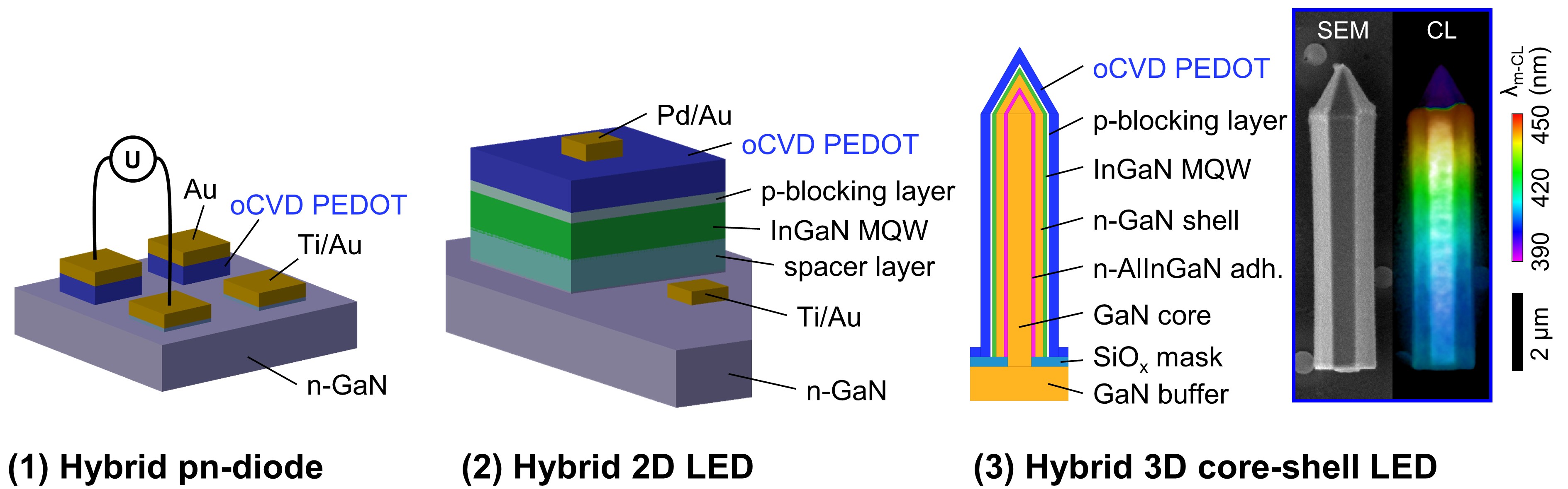
First, 2D reference structures consisting of GaN/oCVD-PEDOT were considered to reveal the electrical characteristics at the hybrid interface. We suggest thermionic emission as the main conduction mechanism and obtained high rectification ratios of up to 107 at ±2 V, low ideality factors of ~2.01, mean barrier heights of ~1.42 eV at room temperature and excellent thermal and temporal stability, a prerequisite for reliable applications in optoelectronics. Therefore, we proceeded in a second step with 2D LED structures featuring an InGaN multi-quantum well (MQW) for blue light emission and compared purely inorganic LEDs (based on state-of-the-art p-GaN) with our hybrid design (based on oCVD PEDOT). We found that the hybrid LED offers pronounced electroluminescence and a substantially enlarged light-emitting area attributed to the advanced current spreading property of the conductive polymer. In the third step, we applied our hybrid concept to a cutting-edge 3D core-shell microrod LED design provided by OSRAM Opto Semiconductors and observed a broad electroluminescence spectrum that indicates light emission from the entire microrod length. From these findings, we conclude that oCVD PEDOT can be a key component in the realization of new hybrid inorganic/organic 3D LEDs based on GaN microstructures.
Follow the Topic
-
Nature Communications
An open access, multidisciplinary journal dedicated to publishing high-quality research in all areas of the biological, health, physical, chemical and Earth sciences.

Related Collections
With Collections, you can get published faster and increase your visibility.
Women's Health
Publishing Model: Hybrid
Deadline: Ongoing
Tumor Microenvironment Crosstalk and Therapeutic Implications
Publishing Model: Hybrid
Deadline: Nov 02, 2026


Please sign in or register for FREE
If you are a registered user on Research Communities by Springer Nature, please sign in