Waveplates go thinner and ultrathin!
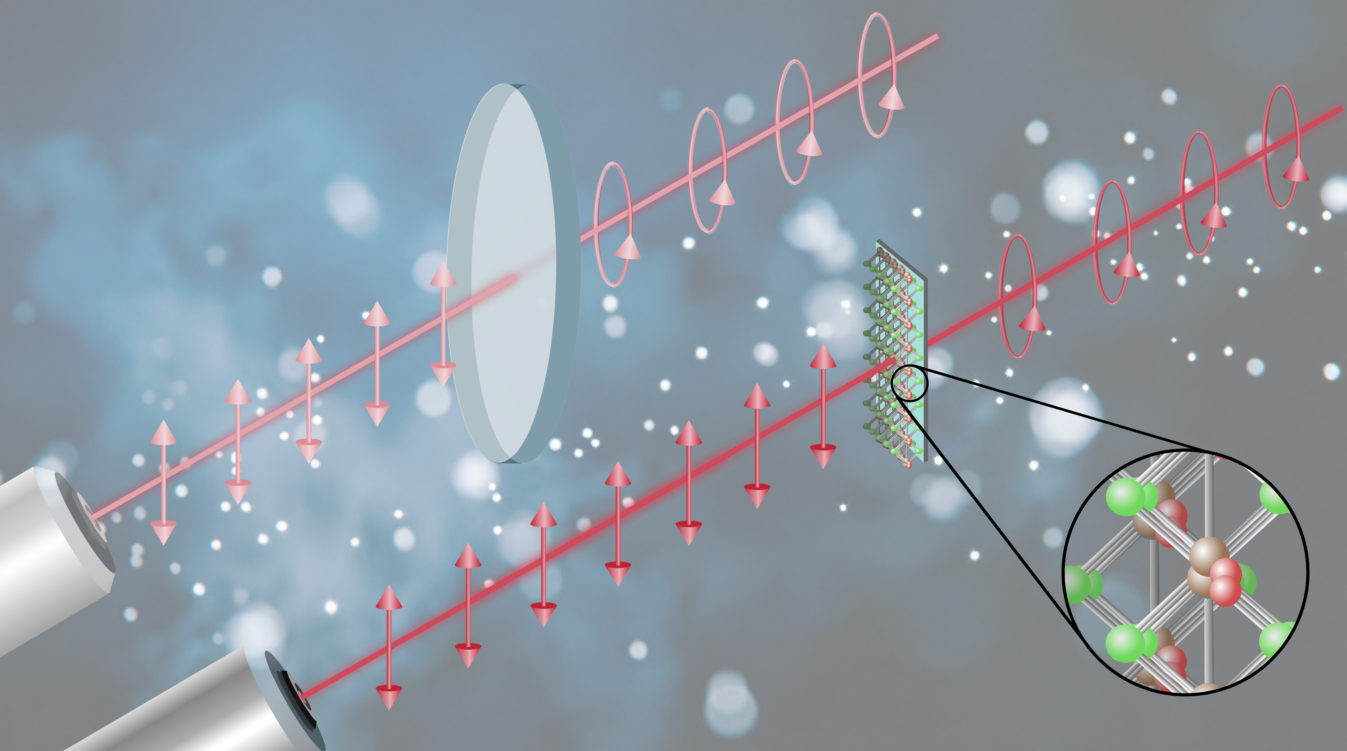
The development of miniaturized waveplates critical for integrated nanophotonics, is currently being limited by "polishing-induced" surface roughness and scattering losses that distort polarization control when commercial birefringent crystals are physically scaled to sub-millimetre dimensions. Shattering these traditional constraints, the introduction of two-dimensional (2D) niobium oxychloride (NbOCl₂) presents a revolutionary class of ultrathin quarter-waveplates (QWPs) that leverages upon the material's pronounced biaxial optical anisotropy.
Fundamental materials characterization of NbOCl2 flakes demonstrates distinct birefringence, along with discernible crystallographic anisotropy shown in its Raman profile. More importantly, the "atomically smooth" van der Waals surface of these crystal flakes achieved sub-nanometre RMS roughness—less than 0.1% of the device thickness, paving a crucial characteristic for NbOCl₂ to bypass the need for costly industrial process that would prove to be detrimental to the crystal's optical fidelity at reduced dimensions.
 for multiple NbOCl2 samples tabulated from AFM measurements. d, e, Polarized Raman intensity mapping of NbOCl2 sample as a function of wave number and sample angle under cross and parallel polarization configurations. f-h, Polar plots of the measured and fitted peak (P1, P3, P5) intensities under the respective polarization configurations (cross or parallel).")
Figure 1. Crystal orientation determination. a, Optical images of NbOCl2 nanoflake under cross-polarizer setup. The white and orange arrows in the figure indicate the polarization directions of the polarizer and analyzer, respectively, with the scale bars of 50 µm. b, Corresponding reflected light intensity as a function of sample rotation angle θ under crossed polarization conditions. c, RMS surface roughness (Rq) for multiple NbOCl2 samples tabulated from AFM measurements. d, e, Polarized Raman intensity mapping of NbOCl2 sample as a function of wave number and sample angle under cross and parallel polarization configurations. f-h, Polar plots of the measured and fitted peak (P1, P3, P5) intensities under the respective polarization configurations (cross or parallel).
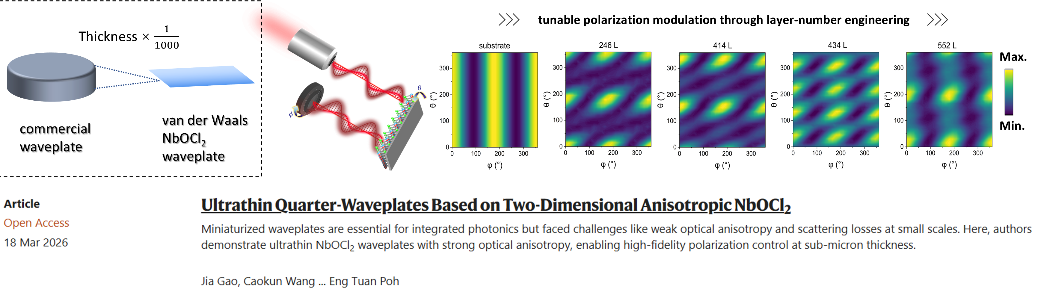
Across a series of sample with differing thicknesses, the evolving spectra profiles derived various metrics of optical anisotropy, such as the dichroic ratio and ellipticity of the crystals that allows the optimal selection of operating wavelengths (at high ellipticity) corresponding to each sample thickness. This results in a plethora of samples with different thicknesses, each catering to specific wavelength ranges for quarter-wave operations.
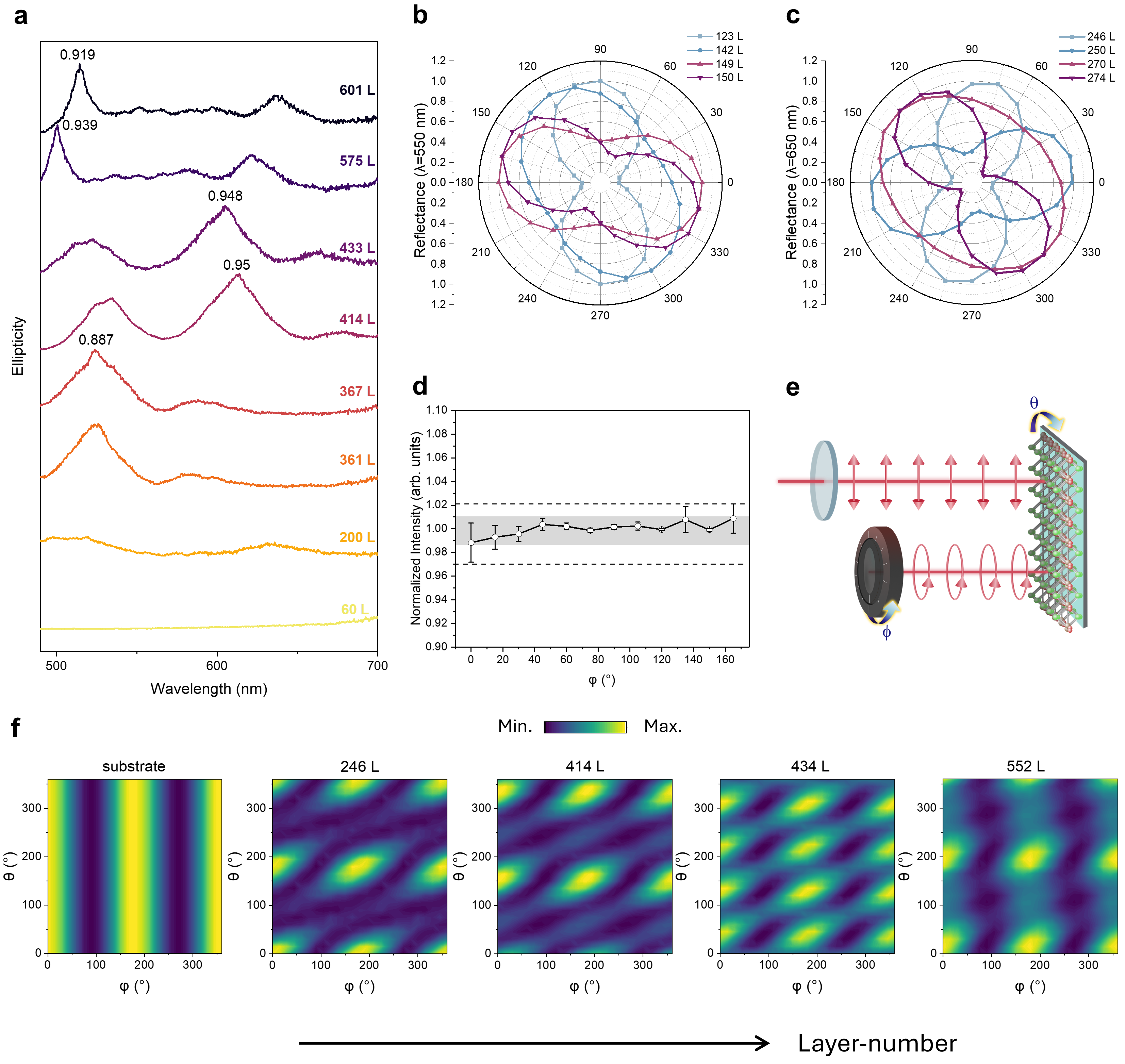
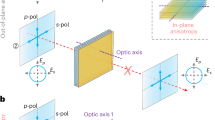
Figure 3. Layer-dependent polarization modulation of NbOCl2 waveplates. a, Ellipticity spectra at different layer numbers. b, c, Polar plots of NbOCl2 flakes with different layer numbers at wavelengths of 550 nm and 650 nm, respectively. d, Variation of normalized intensity as a function of analyser angle φ under 45° illumination (layer numbers: 414 L, wavelength: 614 nm), where error bars represent the standard deviation. e, Schematic diagram of the polarization modulation setup. f, Different layer-number NbOCl2 reflective intensity under the change in sample angle and analyser angle at 652 nm. Layer numbers are shown above each figure.
With a specified laser wavelength, samples of varying thicknesses can be screened of their polarization modulation profile for elliptical profiles that resembles the polarization behavior of an ideal quarter-waveplate. The demonstrated matching pairs (d = 269 nm, λ = 614 nm; d = 282 nm, λ = 605 nm; d = 374 nm, λ = 500 nm) with identical profiles compared against the theoretical polarization modulation for a quarter-waveplate, provide strong evidence that a broad selection of operating wavelength ranges can be accessible simply by tuning the thickness of the NbOCl2 samples.
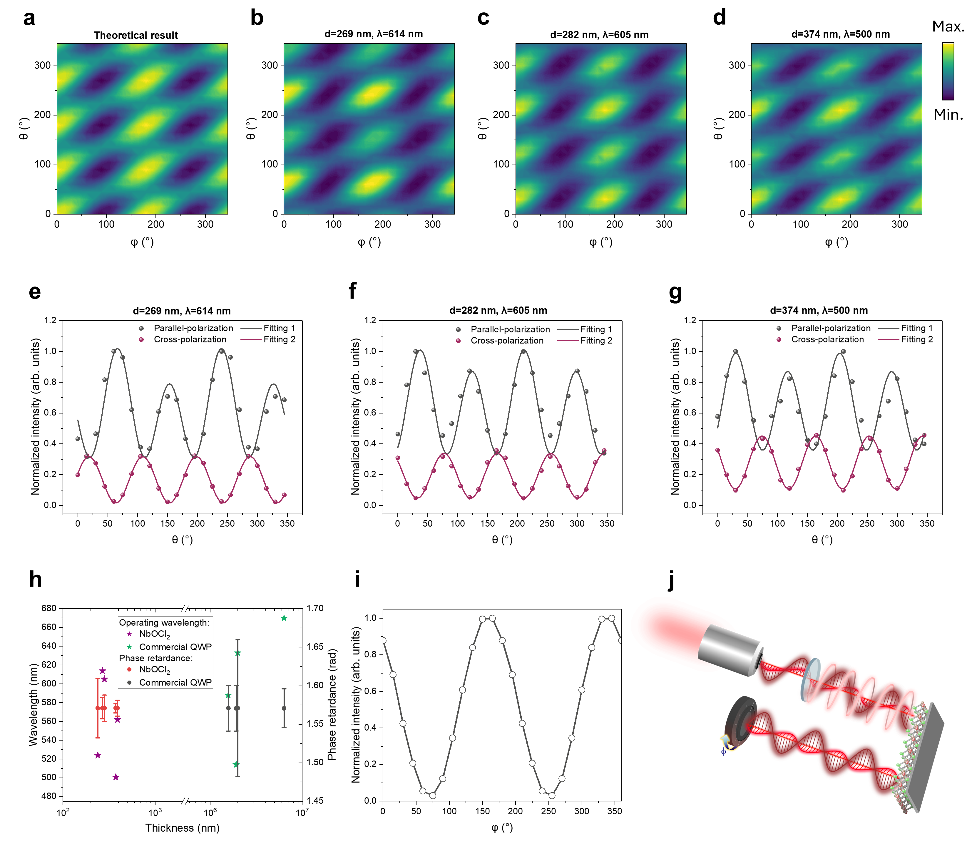
Figure 4. QWP based on NbOCl2. a, Fitting results showing polarization modulation for an ideal QWP. b-d, Experimental results for polarization modulation in NbOCl2 QWPs, for NbOCl2 flakes of 269 nm (414 L), 282 nm (433 L) and 374 nm (575 L), respectively. e-g, Experimental data and fitting results of the normalized intensity under parallel-polarization (polarizer and analyzer aligned) and cross-polarization (polarizer and analyzer perpendicular) conditions, plotted as a function of the sample rotation angle. h, Performance comparison of NbOCl2 QWPs against commercially available QWPs, inclusive of Thorlabs WPQSM05-514 (514 nm), WPQSM05-588 (588 nm), WPQ05ME-633 (633 nm) and Edmund Optics #49-221 (670 nm). Error bars represent the standard deviation of phase retardance values. i, j, Experimental result and schematic illustration of the modulation measurement for linearly polarized light passing through a QWP and NbOCl₂, whereby the fast axes of the QWP and NbOCl2 are perpendicular to each other.
With a record-thin 269 nm quarter-waveplate operating at 614 nm, the performance could be benchmarked against commercial counterparts, delivering elite phase retardance accuracy (λ/600) that rivals or surpass these bulky commercial waveplates. Finally, with a commercial waveplate of similar operation specifications (~614 nm), the conversion of the resultant circularly polarized light back to a linearly polarized profile ensures performance quality of our ultrathin waveplate.
The tunability of these devices through thickness-dependent modulation positions NbOCl₂ as a foundational platform for the next generation of 2D optics and photonics—a field currently exploding due to the demand for chip-integrated polarization control in quantum systems and fiber-optic communications. By enabling high-fidelity light modulation at a fraction of the traditional footprint, this breakthrough provides the essential hardware for subwavelength, on-chip optical circuits, marking a definitive shift from bulk-constrained components to scalable, 2D-material-based nanophotonic architectures.
The article, along with its associated details is available at https://www.nature.com/articles/s41467-026-70788-3
Follow the Topic
-
Nature Communications
An open access, multidisciplinary journal dedicated to publishing high-quality research in all areas of the biological, health, physical, chemical and Earth sciences.

Related Collections
With Collections, you can get published faster and increase your visibility.
Women's Health
Publishing Model: Hybrid
Deadline: Ongoing
Tumor Microenvironment Crosstalk and Therapeutic Implications
Publishing Model: Hybrid
Deadline: Nov 02, 2026


Please sign in or register for FREE
If you are a registered user on Research Communities by Springer Nature, please sign in