2D Schottky junction device reveals optoelectronic reconfiguration concept
Why this research matters
The dramatic expansion of artificial intelligence and big data is driving demand for increasingly sophisticated and faster-evolving electronic product functionalities, fundamentally reshaping human life in many ways. Moore's Law has guided this progress by predicting the continuous miniaturization of transistors. This scaling down has historically enabled the development of more powerful, energy-efficient, and affordable devices. However, traditional electronics based on metal-oxide-semiconductor field-effect transistors are now facing fundamental physical limits. So, to keep technology advancing, we need devices that can achieve more complex functions much more efficiently. Reconfigurable logic devices present a promising pathway towards this goal. These are devices whose core operational behavior can be dynamically tunned — switching between distinct states to achieve different functionalities on demand. The key benefit lies in potentially requiring fewer physical components to accomplish a given set of functions. Conventional silicon transistors, on the other hand, are inherently limited: fabricated as either N-type or P-type through irreversible doping processes, their function is immutably defined at fabrication. To overcome these limitations, exploration of novel materials and disruptive device architectures is essential.
Our research and findings
Since its exfoliation in 2004, graphene has been recognized for its exceptionally high conductivity and atomic-scale thinness. This discovery sparked extensive research into 2D materials. These materials hold great promise for next-generation electronics because of their ultra-thin dimensions, which allow electric fields to easily control them. Additionally, their strong light-matter interactions and excellent photoresponse make them highly suitable for fabricating optoelectronic devices. Crucially, ambipolar 2D semiconductors like MoTe2 and WSe2 can conduct both electrons and holes, depending on the applied gate voltage. This property is essential for achieving polarity reconfigurability. By leveraging the unique properties of 2D materials, we can dynamically alter a device's function after manufacturing by applying different optical or electrical signals. Our research found that simple all-2D Schottky junctions exhibit behaviors difficult to achieve with traditional silicon transistors. These include reversing rectification direction with gate voltage, switching channel polarity with drain bias voltage, and modulating photoresponse under gate voltage control. Based on these findings, we believe combining optical and electrical control in such junctions can overcome the fundamental limitations of traditional devices, enabling truly reconfigurable optoelectronic devices.
Reconfigurable behaviors
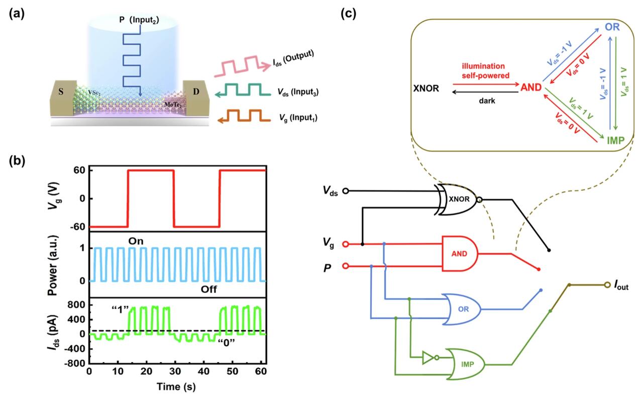
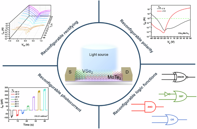
We have selected ambipolar MoTe2 as the channel material due to its superior photoresponsivity and the ability to flexibly tune its Fermi level with gate voltage. To minimize interfacial defects while maintaining high conductivity, we used metallic 2D VSe2 as electrodes instead of conventional 3D metals. Both materials were prepared via mechanical exfoliation and assembled into an all-2D Schottky junction using a dry transfer method. By modulating the gate voltage, drain bias voltage, and optical illumination together, we have observed several reconfigurable phenomena:

Gate-tunable rectifying behavior: In the VSe2/MoTe2 heterostructure, the direction and intensity of the rectification can be significantly changed by applying gate voltages. This tunability arises from gate-tunable band alignment in the 2D heterostructure, which correspondingly modulates the interfacial built-in electric field governing carrier transport.
Dynamic polarity conversion: The VSe2/MoTe2 heterostructure enables dynamically reconfiguration between N-type and P-type transistor operation within a single device. This bias voltage-controlled polarity switching reduces the number of components required in the circuits, which greatly reduces circuit complexity.
Reconfigurable photoresponse: Combining electrical reconfigurability with the excellent light absorption properties of 2D materials, the direction and magnitude of photocurrent can be changed by applying gate voltage and bias voltage.
Reconfigurable logic function: The VSe2/MoTe2 Schottky junction demonstrates superior functional versatility by replacing multiple conventional logic devices with a single unit. This greatly reduces circuit complexity and chip area, enabling more functionality in a smaller space. We have achieved basic logic gates, including XNOR, AND, OR, and IMP, using significantly fewer transistors than traditional silicon circuits. The device can dynamically change its function under different photoelectric inputs, adapting to different computing needs or operating conditions, and provide unprecedented flexibility.
Future directions
2D materials, with their unique atomic-scale properties, are revolutionary building blocks for next-generation electronics. All-2D Schottky junctions represent a critical step towards highly efficient and multifunctional components. Moving forward, our research will shift focus from laboratory-scale device fabrication to realizing large-scale integrated circuits. We aim to push optoelectronic technologies towards greater miniaturization, faster speed, enhanced functionality, and lower power consumption. We anticipate broad applications in flexible electronics, secure circuits, and sensor-integrated image processing systems, achieving significant practicality without compromising performance.
Follow the Topic
-
Communications Materials
A selective open access journal from Nature Portfolio publishing high-quality research, reviews and commentary in all areas of materials science.

Related Collections
With Collections, you can get published faster and increase your visibility.
Materials for quantum sensing and computing
Publishing Model: Open Access
Deadline: Jul 09, 2026
Lead-free perovskite solar cells
Publishing Model: Open Access
Deadline: Jul 08, 2026


Please sign in or register for FREE
If you are a registered user on Research Communities by Springer Nature, please sign in