3D Printed Silica with Nanoscale Resolution
Published in Electrical & Electronic Engineering

Silica is one of the most widely used inorganic materials that demands fabrication methods with nanoscale resolution in fields such as micro-electronics, micro-electro-mechanical systems and micro-photonics. To fabricate silica with des
ired nanostructures, complicated top-down fabrication methods are normally required. Although mature processing techniques with high yield have been developed, these techniques involve the use of hazardous chemicals and complex facilities for fabrication. Moreover, achieving intricate and/or asymmetric 3D architectures at nanometer resolution is very challenging using top-down fabrication methods.
The emerging technology of additive manufacturing, or 3D printing can simplify fabrication processes and create complex architectures, such as curvilinear substrates, nonplanar surfaces, and tortuous 3D patterns, which are beyond the capability of traditional top-down patterning methods. However, there are two facts hinder the application of 3D printing. First, the relatively low spatial resolution offered by commercial 3D printing techniques limits their applications in micro-electronics, MEMS, and micro-photonics. Second, most of 3D printing techniques are designed for polymers. Although very few 3D printing techniques utilizing hybrid organic-inorganic materials and polymer-derived ceramics have been developed, the final parts often contain mixtures of carbon or nitrogen elements that present less controllable electrical properties and lack optical transparency. This hinders their applications in microelectronics and micro/nano-photonics.
To address these limitations, we propose an approach to 3D print silica nanostructures with sub-200 nm resolution. The technique involves 2PP enabled 3D printing of well-dispersed poly (ethylene glycol) (PEG)-functionalized colloidal silica nanocomposite ink, followed by pyrolysis and sintering, where the post-processing procedure determines the crystallinity of the structures produced. In our proposed technique, making a suitable “ink” containing silica nanoparticles (NPs) and two-photon polymerizable precursor is the dominating factor. Such ink must meet several conditions:
- the size of silica NPs has to be small (about 10 nm) to achieve nanoscale resolution;
- the refractive index of the photopolymer precursor must match that of silica to obtain transparent ink to eliminate photo extinction and scattering;
- the heat conductivity of ink must be high to avoid instant vaporization by the femtosecond;
- the ink must be very homogeneous and well-dispersed;
- the mass loading of the silica NPs should be high to maintain the printed geometry and minimize deformation.
Simultaneously meeting all the above conditions is challenging. For example, though using smaller NPs is necessary to achieve high resolution, sub-micron size particles can result in an undesirable mixture with high viscosity, which in turn makes mechanical mixing difficult. Additionally, high viscosity also leads to low heat conductivity because viscosity is normally inversely proportional to heat conductivity. To resolve these conflicts, our strategy is to use PEG-functionalized well-dispersed colloidal silica NPs and the mixture of two small molecule acrylate precursors. The polymer precursors contain the same PEG functional group as colloidal silica NPs, which makes the silica NPs have excellent miscibility and dispersity in the polymer precursors. Moreover, the mixture of polymer precursors has the same refractive index as silica and can be fully removed during the subsequent annealing processes.
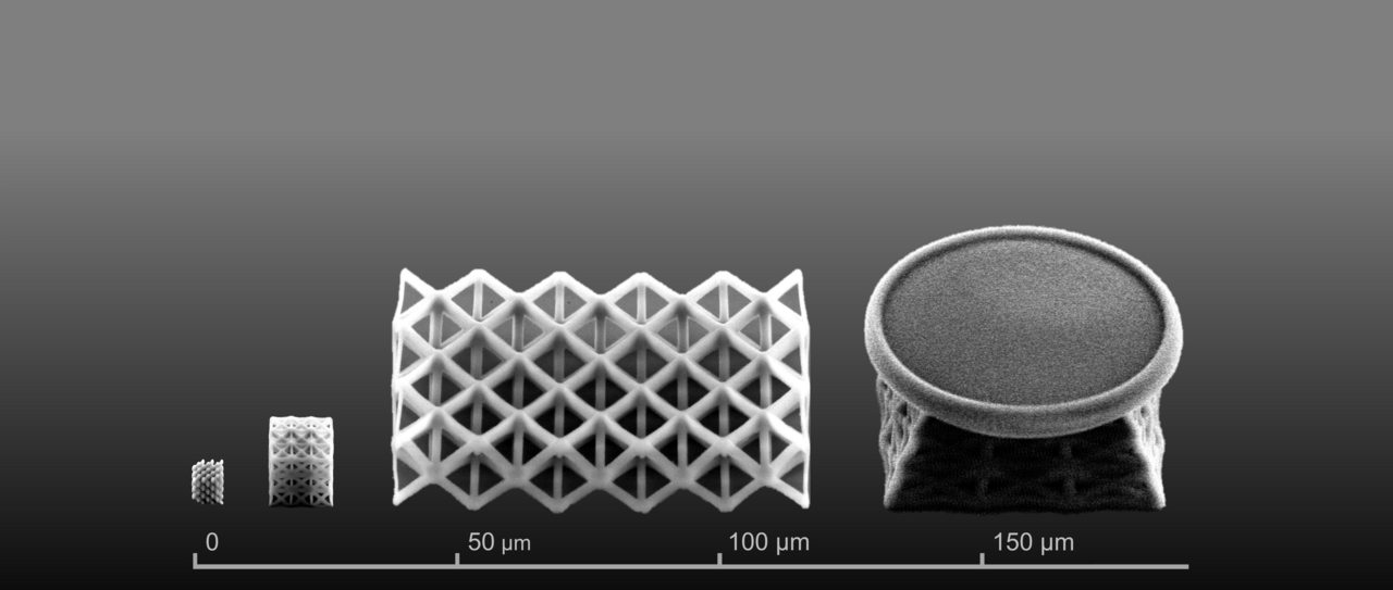
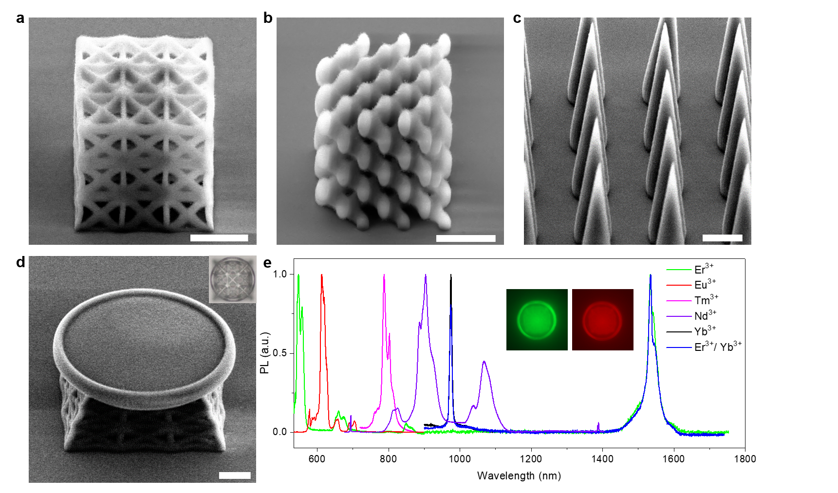
With the successful preparation of the nanocomposite ink and employing 2PP printing technique, we demonstrate that the final 3D printed product is of pure silica with sub-200 nm resolution. Depending on the sintering temperature, the final silica structures can be either amorphous glass or polycrystalline cristobalite, suggesting tunability of the optical properties of the printed structures. From the SEM images, we can see that the intricate structures with sub-200 nm resolution could be nicely created using the above approach. Using nanoscale silica glass, we demonstrated that micro-toroid optical resonators fabricated using the proposed technology have quality factors (Q) over 104. Furthermore, we showed that doping and co-doping of rare earth salts such as Er3+, Tm3+, Yb3+, Eu3+ and Nd3+ can be directly implemented in the printed silica structures. The final doped silica glass nanostructure demonstrated strong photoluminescence at the desired wavelengths. Especially for Er3+, the final printed structures exhibit photoluminescence around 1.55 µm, making the proposed technology a powerful tool for optical telecommunication applications.

Figure 1. SEM images of 3D printed a. FCC lattice truss structure (scale bar 5 μm); b. Diamond lattice truss structure (scale bar 10 μm); c. Needle array (scale bar 10 μm); d. Micro-toroid optical resonator (scale bar: 10 μm), inset: Optical image from the top. e. Photoluminescence of Er3+, Eu3+, Tm3+, Nd3+, Yb3+ doped and Er3+/Yb3+ 1:1 co-doped silica crystal in the visible to near infrared range, inset: showing the Er3+ doped micro-toroid optical resonator under 495 nm (left) and 592 nm (right) excitation and observed at 519 nm (left) and 614 nm (right) using a fluorescence microscope.
This method demonstrates the potential of building passive and active integrated micro-photonic chips with silica via 3D printing. Further work to demonstrate sub-10 nm resolution with stimulated emission depletion methods will bring exciting development to the field. It is also envisioned that arbitrary 3D structure of crystalline silicon can be fabricated by magnesium reduction of printed crystalline silica, making the dream of 3D printing silicon chips a reality.
Follow the Topic
-
Nature Materials

A monthly multi-disciplinary journal that brings together cutting-edge research across the entire spectrum of materials science and engineering, including applied and fundamental aspects of the synthesis/processing, structure/composition, properties and performance of materials.


Please sign in or register for FREE
If you are a registered user on Research Communities by Springer Nature, please sign in