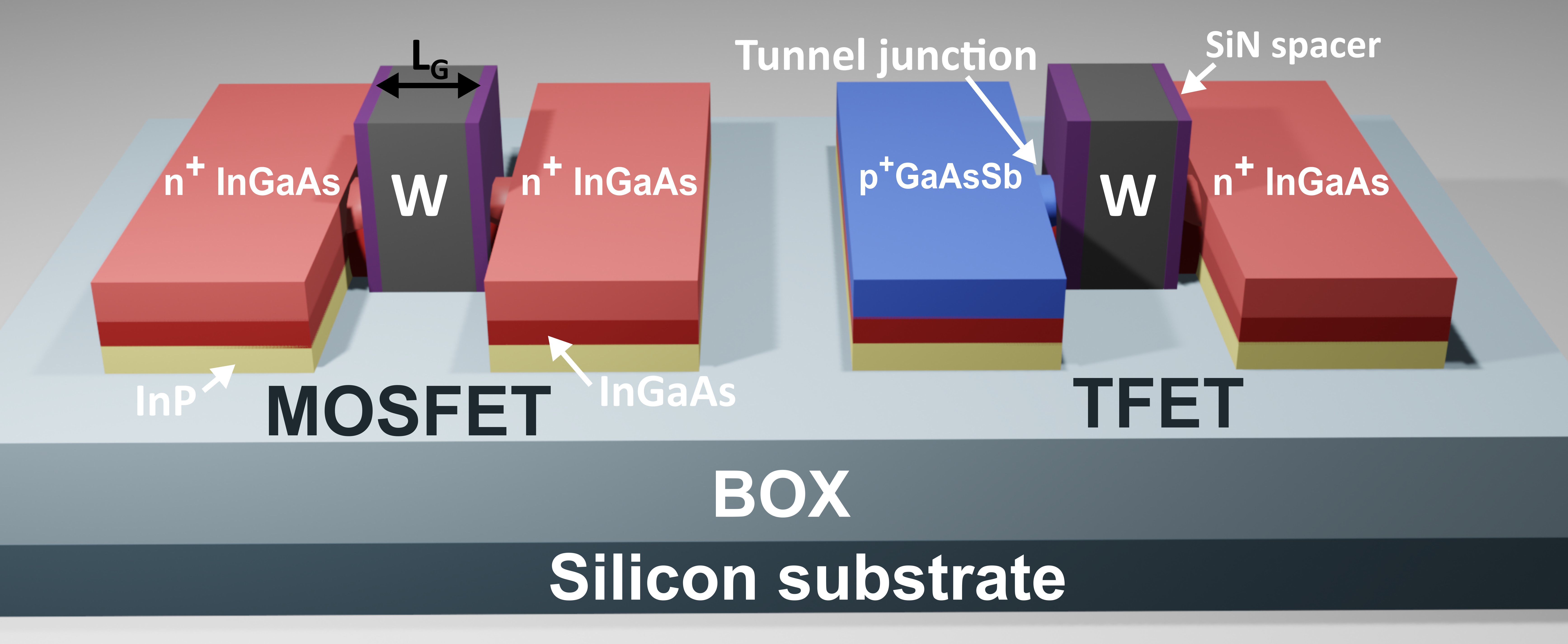
A hybrid technology platform combining tunnel FETs and MOSFETs
In this work we demonstrate an advanced III-V platform which allows for the co-integration of TFETs and MOSFETs. Differentiation at the individual device level is based on a single source re-growth step replacing an InGaAs source of the MOSFET by a GaSb source for the TFET.
Published in Electrical & Electronic Engineering
Like
Liked by Nahush

As Moore’s law is approaching its end, reducing the power consumption of transistors has become the new challenge. It is in fact crucial to increase the energy efficiency of electronics at all levels from system architectures and interconnects down to the individual devices, with the ultimate goal to reduce the carbon footprint of electronics.
The power consumption of electronics is increasingly limiting system performance and simultaneously, massive amounts of data are being generated by the billions of devices we are surrounded by. The generated information needs to be computed, transmitted and stored, increasing the energy consumed by datacenters to an extent that is no longer sustainable by our ecosystem. It is therefore essential to reduce the power consumption of electronics on several fronts, ranging from system architectures and interconnects, down to the individual device level, targeting a reduction of the carbon footprint produced by the ICT industry.
Key to reducing the power consumption of individual components is to reduce the bias voltage at which they operate. This is ultimately limited by the steepness of the transition between “on” and “off“ state – referred to as subthreshold swing: The steeper this transient the less energy is required to turn on/off a transistor. CMOS devices – currently constituting the main building block of electronic circuits – are fundamentally limited by a minimum subthreshold swing of 60 mV/decade at 300 K. This means that for those devices it will ultimately be extremely challenging to reduce the bias voltage beyond the 0.7 V that is seen as the lower limit today. Tunnel field-effect transistors (TFETs) instead, exploit quantum mechanical tunneling to overcome this limitation, hence it is possible to operate these devices at much lower bias levels and with reduced leakage, which can lead to substantial gains in energy efficiency.
Unlike conventional transistors, TFETs have stringent requirements in terms of channel materials, device dimensions and energy band-alignment, hence heterostructures made of III-V compounds are essential to demonstrate superior TFET performance. The tunnel FET unlike a MOSFET is a junction device. Precise alignment of the gate to the tunnel junction is required to achieve simultaneously a steep subthreshold swing and adequate drive current. In this work we demonstrate a scaled TFET platform with sub-50-nm gate lengths in an advanced process, suitable for large scale integration. Key to achieving this is the development of a selective-source approach wherein the GaSb source material is grown only towards the end of the process. The use of digital etching and epitaxial regrowth allows for an accurate alignment with the gate.
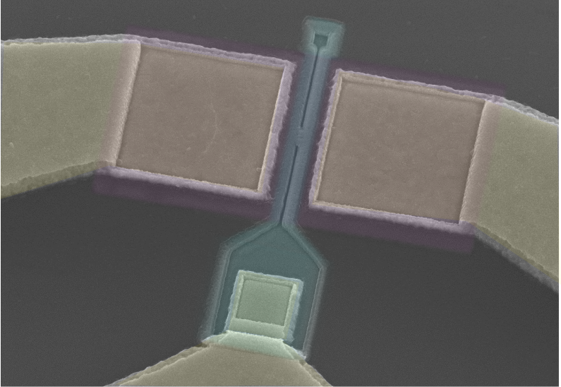
This technique allows differentiating between a MOSFET and a TFET simply by a single masking step. This degree of granularity makes it possible to design logic blocks combining TFETs with lower power consumption and MOSFETs, which are potentially faster and possess higher drive current at higher voltage levels. In this work we demonstrate a scaled III-V hybrid TFET-MOSFET technology on Si which allows for side-by-side fabrication of record-performance TFETs, with a minimum subthreshold swing of 42 mV/dec, and state-of-the-art III-V MOSFETs, with a minimum subthreshold swing of 62 mV/dec. The device platform presented in this work sets a strong premise for future advanced ultra-low-power logic nodes based on hybrid TFET/MOSFET technology.
This work was partially funded by the European FP7 program under grant agreement No. 619509 (E2SWITCH) and by the Horizon 2020 programs under grant agreement No. 688784 (INSIGHT) and 871764 (SEQUENCE).
Multiple Contributors
Follow the Topic
Electrical and Electronic Engineering
Technology and Engineering > Electrical and Electronic Engineering
-
Nature Electronics
This journal publishes both fundamental and applied research across all areas of electronics, from the study of novel phenomena and devices, to the design, construction and wider application of electronic circuits.


Please sign in or register for FREE
If you are a registered user on Research Communities by Springer Nature, please sign in