A Valuable and Low‑Budget Process Scheme of Equivalized 1 nm Technology Node Based on 2D Materials
Published in Materials

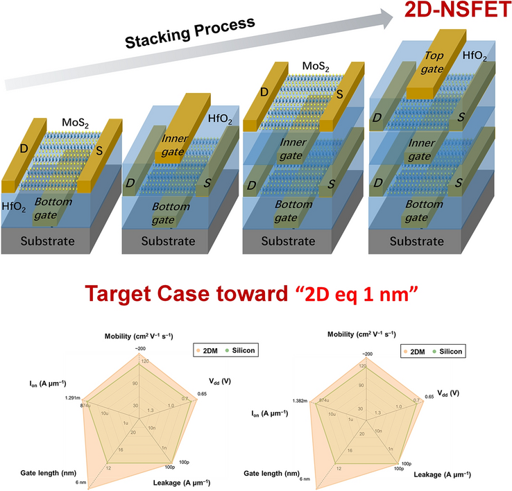
As the IRDS roadmap eyes Si-CFET for the 1 nm generation, the mask count, 3-D stacking and parasitic capacitance required threaten to explode cost and complexity. Now a Fudan–Tsinghua–ECNU team led by Prof. Wenzhong Bao, Prof. Yabin Sun and Prof. He Tian proposes a lateral-scaling alternative: “2D eq 1 nm”—a MoS2 nanosheet-FET (NSFET) flow that needs only half the photomasks and no vertical PMOS/NMOS stacking yet outperforms Si-CFET in power, speed and area.
Why 2D-NSFET Matters
-
Horizontal Scaling Instead of Vertical Stacking
– CGP shrinks from 40 nm (Si-CFET) to 20 nm; L scales to 6 nm while keeping SS ≤ 61 mV dec-1and DIBL ≤ 42 mV V-1—24 mV dec-1 and 78 mV V-1 better than Si at the same gate length. -
36 % Frequency Gain @ Iso-Power
– Calibrated BSIM-CMG ring-oscillator runs 36 % faster than 1 nm Si-CFET and 28 % faster than 3 nm Si-NSFET at identical 0.65 V supply and power. -
Mask-Count & Cost Reduction
– Eliminating CFET’s 3-D integration slashes >50 masks; EUV layers drop from ~18 to ~9, cutting lithography cost by ≈ 40 %. -
Proven Device Uniformity
– Wafer-scale CVD 3-layer MoS₂ arrays deliver I ≈ 1.3 mA μm-1, I ≈ 109and σ(V) < 80 mV across 200 mm substrate.
Cross-Scale Simulation Framework
DFT → TCAD → SPICE → 16-bit RISC-V CPU:
- Material: DFT-computed multi-valley DOS for WS2(electron mass 0.34 m0, ΔE = 0.18 eV) fed into TCAD.
- Device: Quantum-corrected drift-diffusion calibrated against fabricated 6 nm LG MoS2 NSFETs (EOT = 0.9 nm, R = 180 Ω μm).
- Circuit: 15-stage RO and 9-standard-cell library (AOI22, XOR2, MUX21…) synthesized at 0.65 V; extracted C 20 % lower, I 30 % higher than Si-CFET.
- System: Open-source 16-bit RISC-V core shows 48 % frequency boost and 17 % power reduction versus 1 nm Si-CFET at iso-area.
Process Flow & Scalability
- 40 nm-deep trench etch → Au back-gate
- 15 nm ALD HfO2 gate dielectric
- CVD 3-layer MoS2 transfer, litho/etch channel
- Self-aligned 5 nm Ti / 40 nm Au S/D
- Repeat for 2nd nanosheet; 110 nm Au top-gate
- Via etch & metallization connect dual channels
All steps use laser-direct-write lithography (≤ 300 nm overlay) and are foundry-compatible; yield-limiting steps (uniform MoS2 growth, low-R contact) are flagged for ongoing optimization.
Challenges & Outlook
Contact resistance below 150 Ω μm and >900 cm2 V-1 s-1 mobility must co-exist at 6 nm LG to hit the simulated PPA. The team is now integrating semi-metallic Sb contacts and sub-1 nm EOT ZrO2 to close the gap, while foundry partners target 2026 pilot-line insertion at the 3 nm (2D+) node.
By replacing 3-D CFET complexity with atomic-thin lateral scaling, the “2D eq 1 nm” scheme offers a lower-cost, higher-speed route to keep Moore’s law alive—without the Moore’s tax.
Editor of Nano-Micro Letters, which is an Open-Access, peer-reviewed journal reported papers that have at least one dimension ranging from a few sub-nanometers to a few hundreds of micrometers. The journal is published by Springer Nature and indexed by SCI, EI, SCOPUS, Pubmed, etc. The 2025 JCR Impact Factor is 38.5. The 2025 CiteScore is 58.9.
Follow the Topic
-
Nano-Micro Letters
Nano-Micro Letters is a peer-reviewed, international, interdisciplinary and open-access journal that focus on science, experiments, engineering, technologies and applications of nano- or microscale structure and system in physics, chemistry, biology, material science, and pharmacy.


Please sign in or register for FREE
If you are a registered user on Research Communities by Springer Nature, please sign in