Boosting photonic device performance by overcoming the quantum-confined Stark effect
Published in Electrical & Electronic Engineering
The paper in Communications Physics is here: go.nature.com/2wXqYja
Whether we look at the production of photons for illumination or of entangled photons, photonics dramatically alters the world around us. Ongoing efforts to optimize the efficiency of photon emitters enabled us to use devices like wearables and to reduce the power consumption of lighting in these critical times for our global climate.
Already several decades ago, researchers recognized that the efficiency of photon production based on the electron-hole recombination in semiconductors can be increased by bringing the charge carriers closer together. Hence, the double heterostructure was invented confining both charge carrier types in few nm wide areas, e.g., of an LED structure by inserting a second semiconductor material with a smaller bandgap energy into a p-n junction. It was obvious to adapt the double heterostructure technique also for the nitride-based structures used by the Nobel laureates Isamu Akasaki, Hiroshi Amano, and Shuji Nakamura to invent the first blue LEDs. But, nitride-based semiconductors have a major drawback: they exhibit strongly polar crystal structures, which lead to immense built-in electrostatic fields when used in heterostructures.
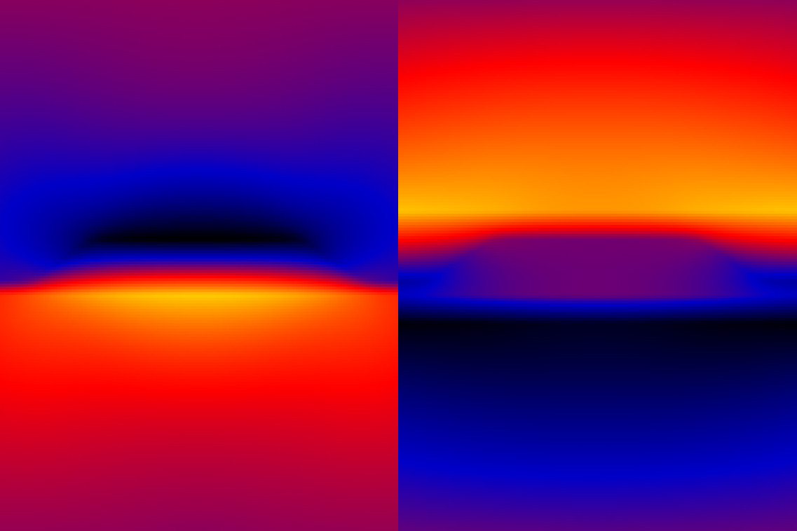
Despite the small dimensions of few nm, the built-in fields are strong enough to separate electrons from holes by squeezing the charge carrier wave functions against opposite potential barriers of the heterostructures, which reduces the recombination probability; and the resulting electric dipole moment of electron-hole pairs within the built-in fields causes a redshift of emitted photon energies. Both, separation and redshift together are commonly termed “quantum-confined Stark effect”, which was already explained by David A. B. Miller et al. after investigating the impact of electrostatic fields applied to double heterostructures in the form of nonpolar quantum wells, years before the invention of blue LEDs.
During the decades after the invention of blue LEDs, there was enough optimization potential in growth processes, doping and LED structures so that the crux of the nitride material system, which are the built-in fields, was not hindering a permanent optimization research. However, already back in 2000, Patrick Waltereit et al. suggested the use of growth planes with normal vector orthogonal to inherent crystal polarization directions for the production of nitride quantum wells “free of electrostatic fields for efficient white light-emitting diodes”.
What sounds like a simple and good idea is, however, not so easy to implement with decent crystalline quality. Furthermore, growth along nonpolar directions is not an option for quantum dots due to their small extent in all three spatial dimensions–and quantum dots suffer very strongly from the quantum-confined Stark effect: While arsenide-based emitters already allow electrically triggered single photon emission rates in the GHz regime, their nitride-based counterparts are slower (by several orders of magnitude) due to the spatial electron hole separation.
However, nitride-based materials have other advantages as they promise a much higher temperature stability, which made nitride quantum dots extremely interesting for my numeric single photon emitter research I started ten years ago in the group of Dieter Bimberg. From that time on, the MV/cm field strengths in GaN/AlN quantum dots were boon and bane for me as they on the one hand allowed novel observations like hybrid-biexciton states but on the other hand reduced the photon emission rates. Hence, it was a very welcome result when Gordon Callsen, Axel Hoffmann, and I made a brainstorming for new research ideas in 2015 and we came up with the simple idea of shielding the built-in polarization fields in nitride heterostructures by themselves, like it can be done within a plate-type capacitor that is enclosed by a second plate-type capacitor.
We called our approach “IFGARD”, which is an acronym for “Internal Field Guarded Active Region Device”. The calculations showed that even for quantum dots, the electron-hole overlap should increase by a factor of 100 (GaN quantum dots in AlN). Something, which would make nitride quantum dots as fast as nonpolar quantum dots from systems with cubic crystal structures, but without the need for cubic phase nitride growth. (Several research groups try to stabilize the cubic phase of nitrides in order to get rid of the detrimental built-in fields within wurtzite crystal quantum dots. IFGARD instead, is based on well-established crystal growth along the most polar c-axis in wurtzite crystals like III-nitrides.)
However, nitride quantum dots are not the only application for IFGARD, as we had developed it with the analogy of plate-type capacitors, the most obvious heterostructure IFGARD can be applied to are quantum wells like in our white LEDs at home. By discussing our approach, we found more and more advantages of IFGARD compared to conventional, polar heterostructures, which forced us to file two IFGARD patents in 2015 and 2016 prior to submitting our IFGARD idea to any journal.
This was a big problem: Try to convince people from your research idea without having any journal publications about this topic—and we needed nitride epitaxy groups in order to get first IFGARD samples for supporting our numeric results experimentally. Our only option was to publish a purely theoretical paper presenting our IFGARD idea in 2017 (arxive preprint in 2016 following the filing of the second patent), which started a quite controversial discussion in the community.
After that publication, we finally found the group of Martin Eickhoff able and willing to grow stacks of IFGARD nanodiscs within nanowires with tapered geometry, which are the perfect testbed for IFGARD as these quantum well-like structures allowed us also to tune the shielding of the built-in polarization field strengths by the taper angle of the nanowires. Luckily, Sarah Schlichting, a former PhD Student in the group of Axel Hoffmann got interested in the IFGARD idea and performed micro-photoluminescence measurements. She found variations of the electron-hole pair lifetimes from 7 µs down to 0.7 ns (factor 10,000) for samples with different taper angles. These results together with Sarah’s other observations published in our paper (https://rdcu.be/42yL) prove, that the IFGARD works and that its impact on the electron hole separation in quantum wells is even larger than what we predicted for quantum dots.
I expect that the IFGARD will inaugurate an entire new field of research on shielded, polar semiconductor heterostructures driven by a set of coincidental IFGARD benefits like temperature and emission color stabilization as well as electric current and light guiding. Furthermore, the advantages of the IFGARD for light emitting, laser, and single/entangled photon diodes (LEDs, LDs, quantum LEDs) will impact sectors of broad interest like:
- molecular-biology (based on DNA manipulation with electrically driven UV-B & UV-C near field quantum LEDs),
- medicine and epidemic control (based on water disinfection and nano-surgery by UV-LEDs & LDs with small footprint),
- quantum information technology (based on high-yield arrays of ultrafast quantum LEDs for the triggered generation of single and entangled photons comprising the wide wavelength range ascribed to, e.g., III-nitrides [UV-NIR])
- physics and material science (based on the novel kind of potential landscape in any polar semiconductor heterostructure, well suited, e.g., for quantum cascade LDs with tuneable band inclinations).
Generally, the IFGARD will enable the true potential of material systems like III-nitrides by eliminating their electrostatic polarization fields. Hence, so far inaccessible wavelength ranges will come into reach, e.g., for ultrafast (GHz) LDs with low threshold or for closing the green gap in LED Efficiency.
Follow the Topic
-
Communications Physics
An open access journal from Nature Portfolio publishing high-quality research, reviews and commentary in all areas of the physical sciences.

Related Collections
With Collections, you can get published faster and increase your visibility.
Advances in Quantum Networking: QKD and beyond
Publishing Model: Open Access
Deadline: Jul 31, 2026
Nonlinear dynamics of living systems
Publishing Model: Open Access
Deadline: Nov 09, 2026

Please sign in or register for FREE
If you are a registered user on Research Communities by Springer Nature, please sign in